Leave Your Message
-
E-mail
-
Whatsapp
-
Message
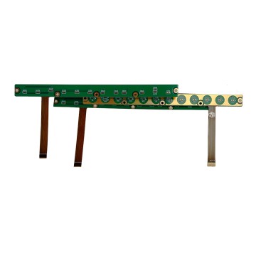
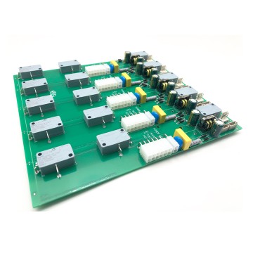
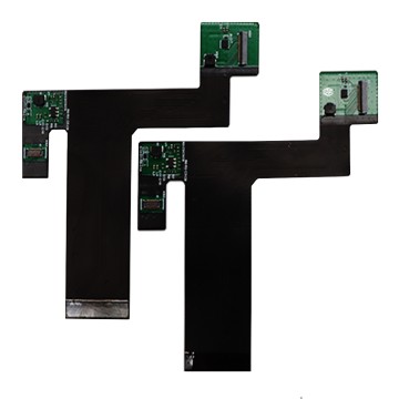
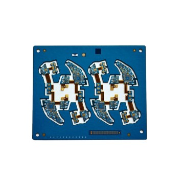
Explore our flagship PCB products engineered for electric vehicle sensor systems and autonomous driving platforms.
As the global electric vehicle (EV) industry accelerates toward full autonomy, the printed circuit board (PCB) has emerged as one of the most mission-critical components in the entire vehicle architecture. An Electric Vehicle PCB for Autonomous Driving Sensors is a highly specialized electronic substrate that forms the core of perception, computation, and communication within self-driving systems. These boards must simultaneously handle high-frequency signal transmission, thermal management, EMI shielding, and mechanical resilience — all within the compact, weight-sensitive confines of a modern EV.
Autonomous driving sensors — including LiDAR (Light Detection and Ranging), millimeter-wave radar, ultrasonic sensors, high-resolution cameras, and infrared detectors — each generate enormous volumes of real-time data. The PCBs that underpin these sensors must process, route, and transmit these signals with near-zero latency and absolute reliability. A single PCB failure in a sensor array can compromise the vehicle's entire perception layer, making manufacturing quality and design precision non-negotiable.
In autonomous vehicles, sensor PCBs operate in extreme temperature ranges (-40°C to +125°C), high-vibration environments, and must maintain signal integrity at frequencies exceeding 77 GHz for radar applications. Multi-layer HDI and rigid-flex PCB designs are now standard for Tier-1 automotive suppliers worldwide.
The design of EV sensor PCBs involves intricate multi-layer stackups — often ranging from 8 to 20 layers — to accommodate the dense routing required by sensor fusion processors and ADAS (Advanced Driver Assistance Systems) chipsets. Materials such as Rogers RO4350B, PTFE-based laminates, and high-Tg FR4 are commonly selected for their superior dielectric properties and thermal stability at automotive-grade operating conditions.
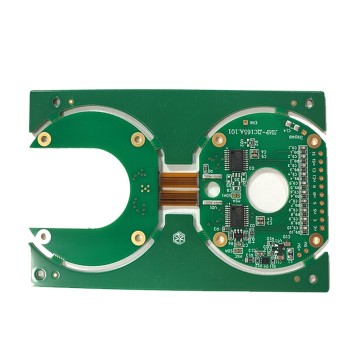
Furthermore, the integration of rigid-flex PCB technology allows sensor modules to be mounted in curved, space-constrained locations throughout the vehicle — from front bumper radar arrays to roof-mounted LiDAR units — without sacrificing electrical performance or mechanical durability. This convergence of advanced materials science, precision manufacturing, and intelligent design is what defines the modern EV sensor PCB landscape.
Industry data reflecting the explosive growth of autonomous driving electronics manufacturing.
The autonomous driving revolution is reshaping PCB design, materials, and manufacturing at every level.
Modern autonomous vehicles rely on the fusion of LiDAR, radar, camera, and ultrasonic data. PCBs must support high-speed SerDes interfaces (LVDS, FPD-Link III) and multi-domain power delivery to process all sensor streams simultaneously.
High-power sensor processors generate significant heat. Embedded heat pipes, metal-core PCBs, and thermally conductive prepregs are increasingly adopted to maintain stable operation across automotive temperature ranges.
Rogers, PTFE, and hybrid laminates are replacing standard FR4 in radar and LiDAR sensor boards. These materials offer low Dk/Df values essential for 77GHz and 120GHz automotive radar signal integrity.
High-Density Interconnect (HDI) with stacked microvias enables the ultra-compact routing required by ADAS SoCs and AI inference chips in autonomous vehicles. Any-layer HDI is now standard for Level 3+ systems.
With dozens of sensors transmitting simultaneously, EMI management is critical. Multi-layer ground planes, embedded shielding structures, and controlled-impedance routing protect signal integrity in noisy EV electrical environments.
AI-powered EDA tools are accelerating PCB layout optimization for sensor boards, automatically routing high-speed differential pairs, managing via stubs, and predicting thermal hotspots before prototyping begins.
From front-facing radar to in-cabin monitoring, EV sensor PCBs enable every layer of autonomous perception.
LiDAR sensors generate millions of 3D data points per second. The PCBs within LiDAR units must support high-speed FPGA or SoC interfaces, precision analog front-ends for time-of-flight measurement, and robust power regulation — all in a thermally demanding rotating or solid-state mechanical housing.
Automotive radar operates at 77GHz for long-range detection and 79GHz for short-range corner radar. These boards require Rogers RO4350B or similar low-loss laminates, precision microstrip transmission lines with tight impedance tolerances (±5%), and hermetic sealing for all-weather reliability.
Surround-view camera systems require flexible PCBs (FPCs) that can route high-resolution MIPI CSI-2 or GMSL2 video signals from multiple camera positions to a central domain controller. Rigid-flex designs allow cameras to be integrated into door mirrors, bumpers, and A-pillars with minimal connector count.
Parking assist and low-speed maneuvering systems use arrays of 8–16 ultrasonic sensors. Their PCBs must manage precise pulse timing, analog signal conditioning, and CAN/LIN bus communication — all in a compact, waterproof package suitable for bumper integration.
The CDC is the brain of the autonomous driving system, fusing all sensor inputs and executing AI inference. These boards feature the highest layer counts (16–20 layers), DDR5 memory interfaces, PCIe Gen5 routing, and advanced power delivery networks for automotive-grade AI accelerator chips.
Driver monitoring systems (DMS) using near-infrared cameras and V2X (Vehicle-to-Everything) communication modules require specialized PCBs supporting 5.9GHz DSRC or C-V2X protocols, integrated antenna structures, and secure communication chipsets for real-time traffic coordination.
The commercial ecosystem surrounding EV PCBs for autonomous driving sensors is experiencing unprecedented consolidation and investment. Global Tier-1 automotive suppliers — including Bosch, Continental, Aptiv, Mobileye, and Valeo — are all scaling up their sensor PCB procurement, with many shifting toward vertically integrated supply chains to ensure quality control from laminate to final assembly.
IATF 16949 certification is the global benchmark for automotive PCB manufacturing quality. It mandates rigorous process controls, traceability, FMEA analysis, and continuous improvement systems — essential for any PCB supplier serving the autonomous driving sensor market. Richpcba holds IATF 16949 certification, ensuring every board meets automotive-grade requirements.
China has emerged as the world's dominant manufacturing base for EV sensor PCBs, accounting for over 55% of global automotive PCB output. Shenzhen, in particular, has developed a dense ecosystem of PCB manufacturers, laminate suppliers, component distributors, and EMS (Electronics Manufacturing Services) providers that enables rapid prototyping, competitive pricing, and high-volume production ramp-up — critical advantages for EV OEMs racing to bring autonomous platforms to market.
Chinese PCB manufacturers serving the automotive sector have made substantial investments in automated optical inspection (AOI), X-ray inspection, impedance testing, and reliability testing infrastructure. Leading manufacturers now offer 24-hour prototype turnaround for sensor PCBs, with full automotive-grade quality documentation including IPC-A-600 Class 3 compliance, material traceability reports, and PPAP documentation for production parts approval.
Automotive OEMs and Tier-1 suppliers impose stringent technical requirements on PCB vendors: minimum trace/space of 3/3 mil for HDI boards, via-in-pad technology for BGA components, controlled-depth back-drilling to eliminate via stubs at high frequencies, laser-drilled microvias with 0.1mm diameter, and surface finishes such as ENIG, ENEPIG, or immersion silver for reliable solderability in automated SMT lines.
Beyond technical specifications, supply chain resilience has become a top commercial priority following semiconductor shortages and geopolitical disruptions. EV manufacturers now demand dual-source PCB qualification, strategic inventory buffers, and real-time production visibility — driving PCB suppliers to invest in MES (Manufacturing Execution Systems) and digital supply chain platforms.
Based in China and looking at the global market, Shenzhen Rich Full Joy Electronics Co., Ltd. has been committed to industry development for 20 years. The company is a national high-tech innovative enterprise that combines focus and expertise. It's also an important enterprise incubation base in China. We specialize in providing customers with one-stop intelligent electronic manufacturing services, including scientific research, PCB design, PCB manufacturing, PCB assembly (including SMT, DIP, Programming and testing) and component selection.
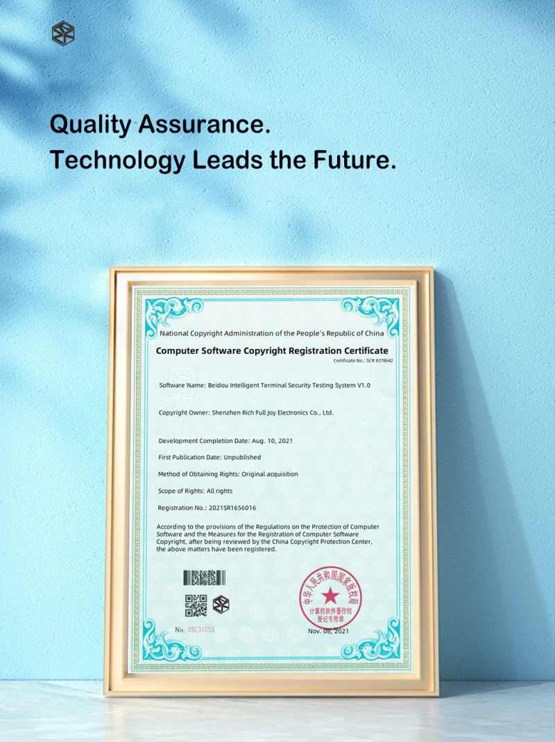
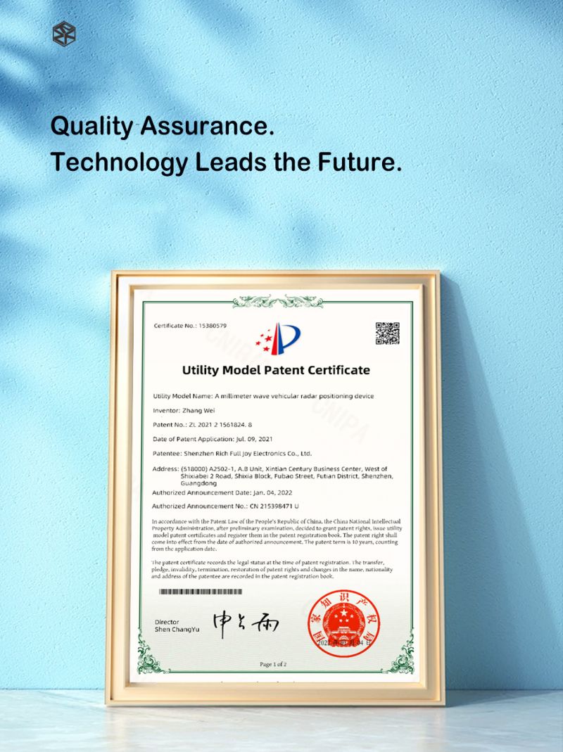
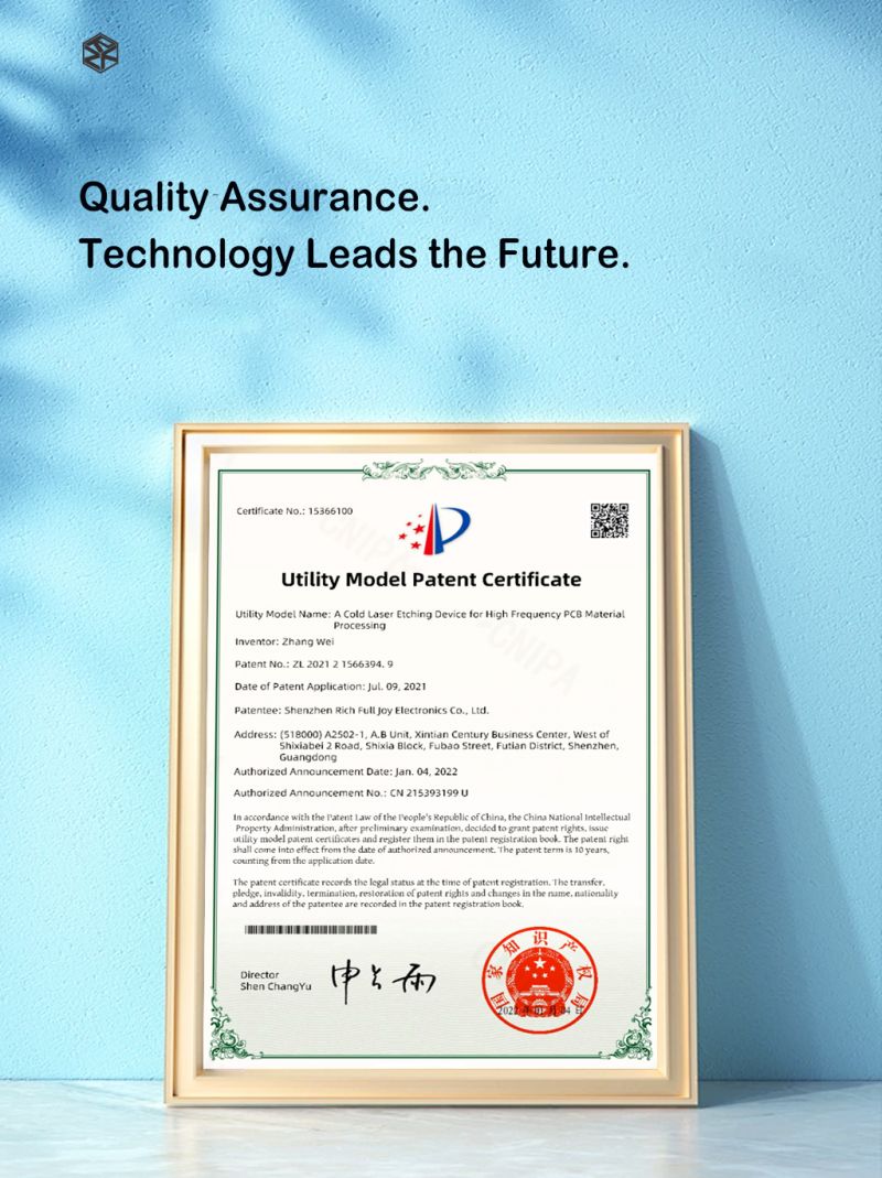
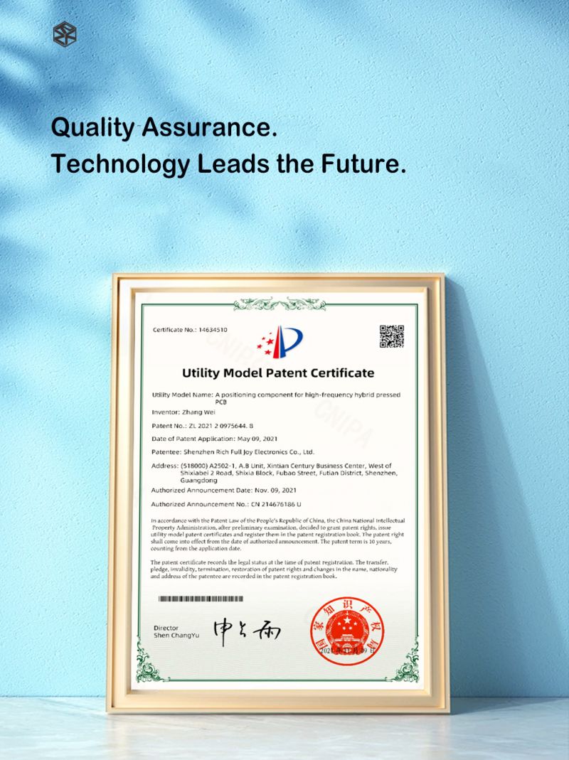
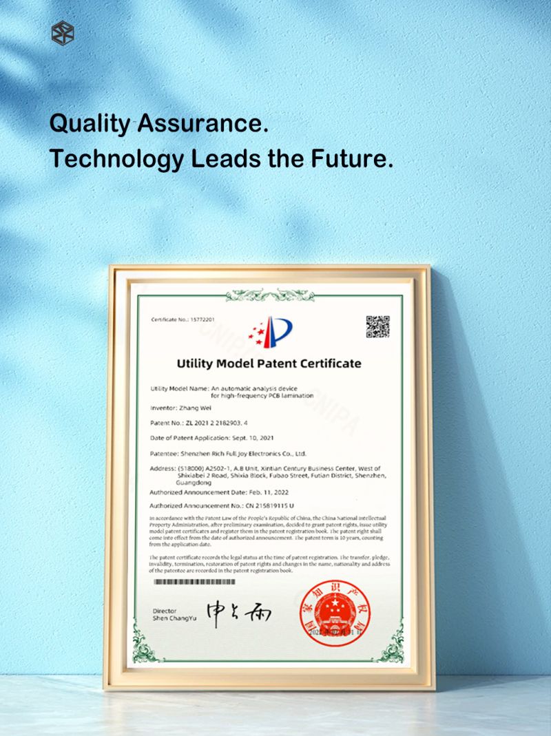
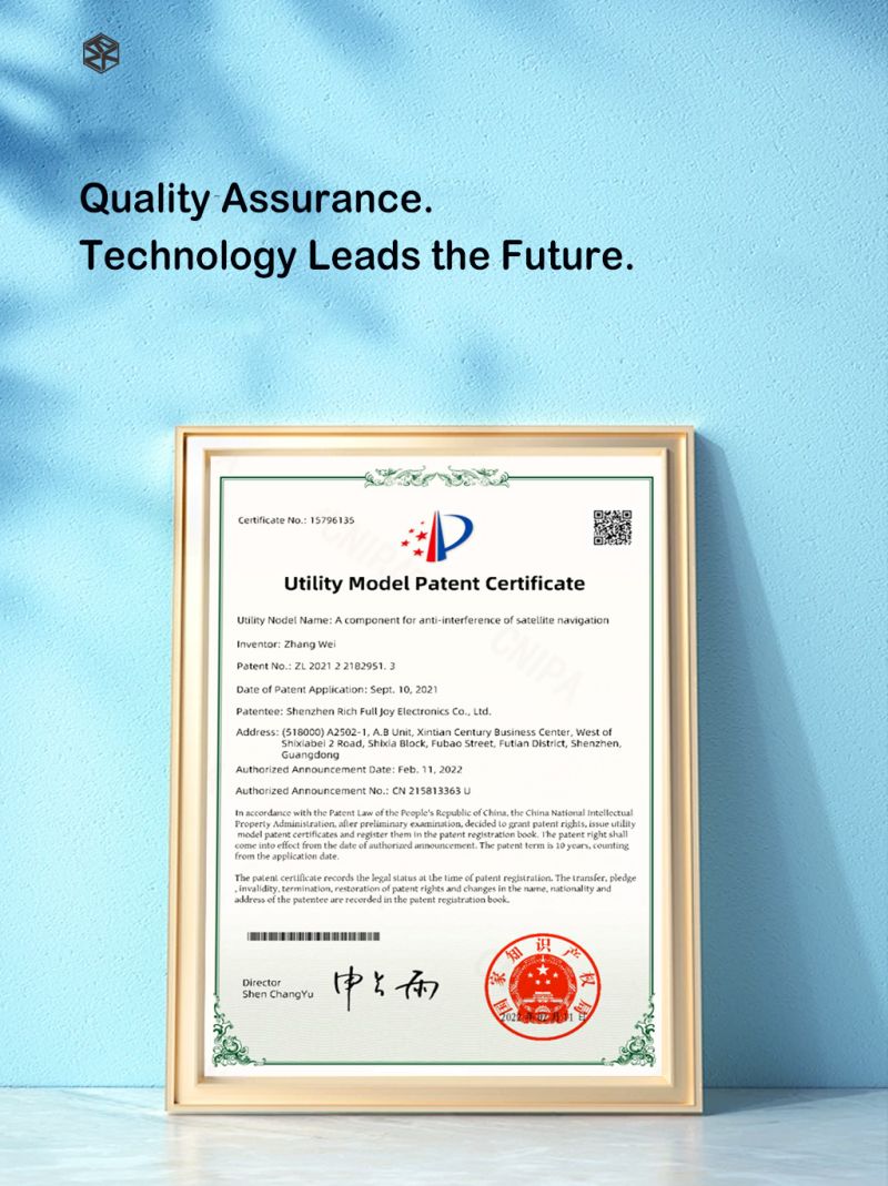
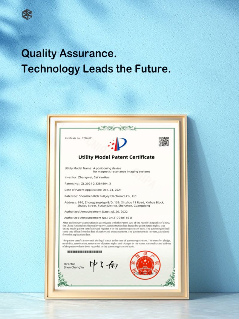
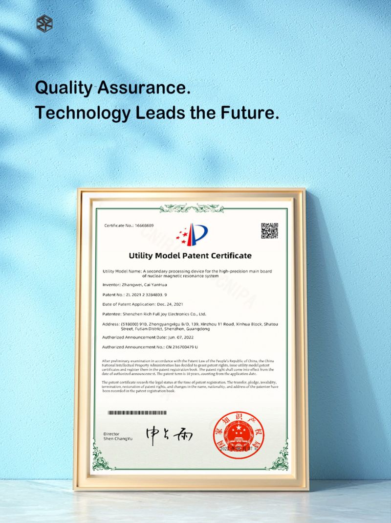
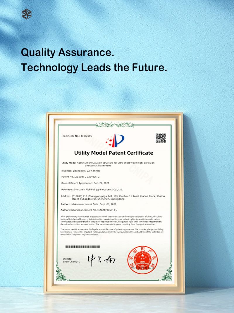
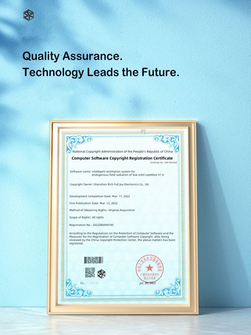
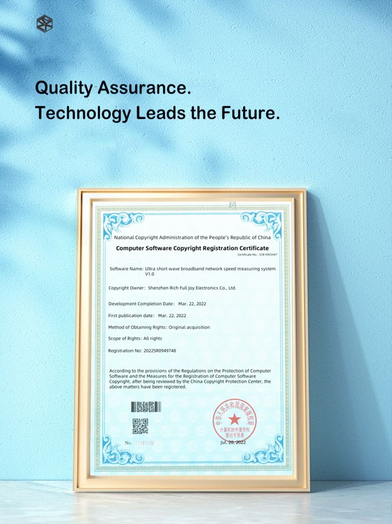
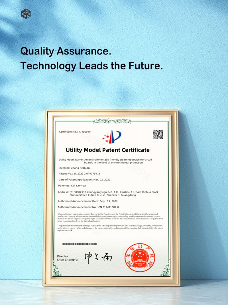
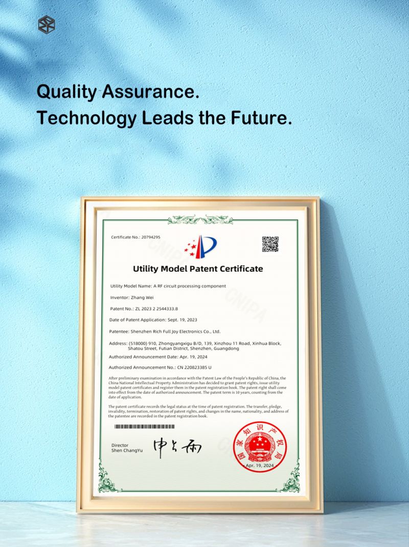
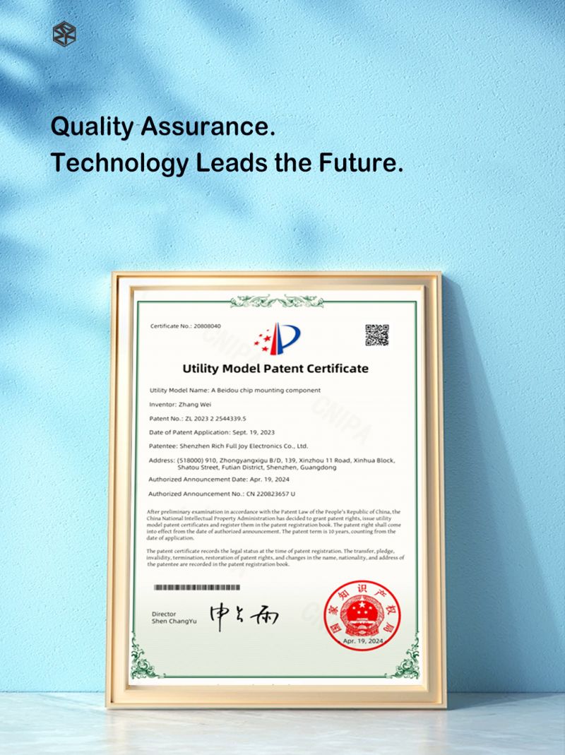
Technological innovation is the core competitiveness of enterprises. We've obtained multiple invention and utility model patents, and has passed various international standard certifications such as ISO9001, IATF16949, ISO14001, UL, CQC, REACH, RoHS, COC, as well as the GJB9001C-2017 standard certification for weapon and equipment quality management system. We've provided high-quality and reliable products to multiple research institutions, universities, and assisted customers in identifying design issues and providing reasonable suggestions and processing parameters.
We not only publish technical papers, but also actively participate in domestic and overseas technology exchange conferences to spread academic value and cutting-edge technological innovation. We regularly communicate with customers and strive to provide them with the best solutions.
Our intellectual property portfolio reflects decades of R&D investment in advanced PCB and sensor technologies.


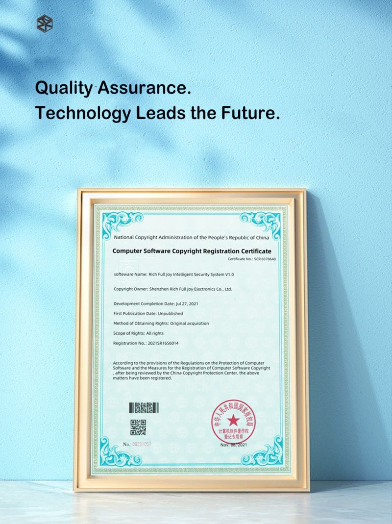
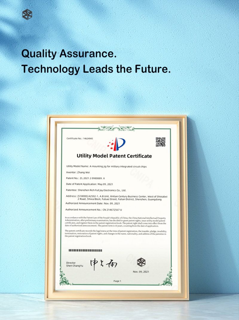
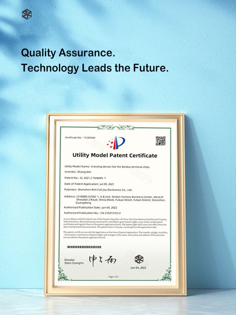



Discover our full range of PCB solutions designed for autonomous driving, new energy vehicles, and advanced sensor applications.