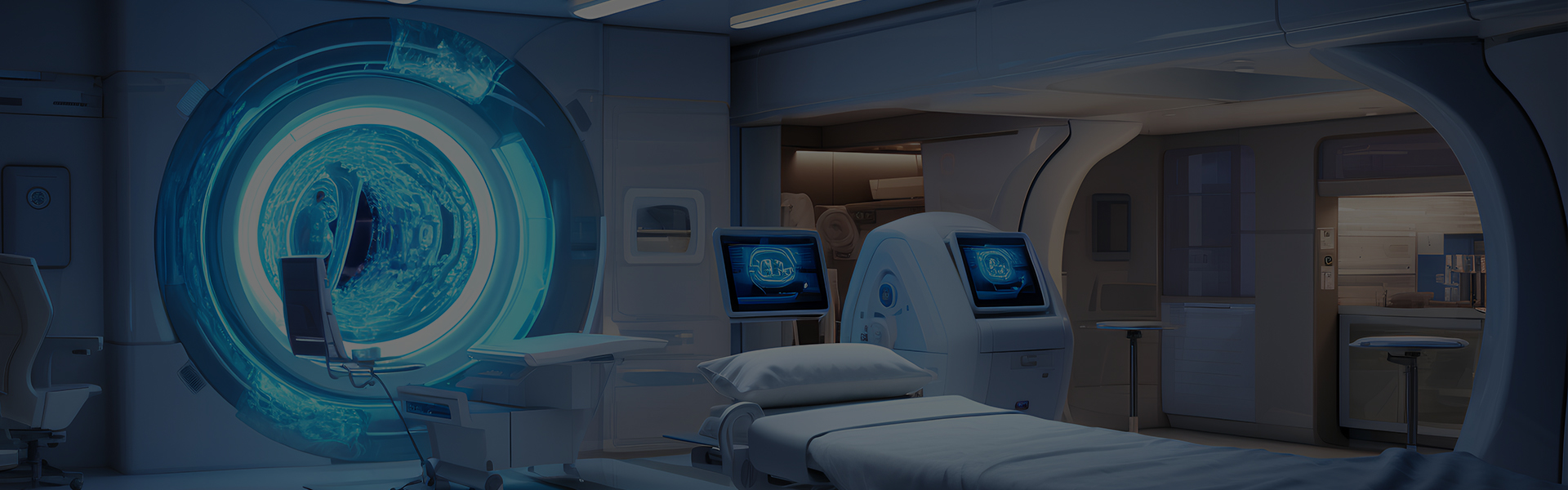
Medical PCB is a specific type of PCB used in the medical industry. As China’s medical industry shifts from traditional Chinese medicine to Western medicine, the demand for medical electronics has dramatically increased. This has prompted the development of China’s medical PCB manufacturing and assembly technology, making RICH PCBA a reliable medical equipment PCBA manufacturer. The medical circuit produced by RICH PCBA is widely used in a range of medical devices, including ultrasound machines, patient monitoring equipment, medical imaging systems, and other devices that require precise and reliable electronic control. These PCBA play a crucial role in controlling and regulating the electronic functions of medical equipment.
Get a Medical PCB Assembly Quote from RICH PCBA
If you’re looking for a top-tier manufacturer of medical PCB/PCBA, go no further than RICH PCBA. Since medical electronics are related to human health, they must meet strict safety and reliability standards. In addition, some implantable medical electronics require greater accuracy and stability, so they need to be designed to withstand harsh medical environments, more testing is involved in manufacturing, and soldering of components needs to be ensured during assembly quality etc.
● Quick Turnaround
● Turnkey PCBA
● Semi-Turnkey
● BGA Assembly
● Prototyping
● Batch Production
● Cheap
● China
What medical electronic PCB have been produced?
Since the outbreak of the COVID-19 pandemic, the global demand for medical electronics has remained high. In this environment, RICH PCBA has received many inquiries from the medical industry. Currently, the majority of the medical PCBA we produce are for electronic forehead thermometers. However, we also manufacture PCBA for other medical devices such as CT scanners, surgical lights, and a range of other products. The following are some examples of the PCBA for medical products that we can provide to our customers:
● Pacemakers
● Defibrillators
● Respirators
● Nursing Monitor
● Electric Wheelchair
● Digital Nutrition Pumps
● MRI Equipment
● Patient Locator
● Cochlear Implants
● Scanning Technology
● Control Systems
● Insulin Pumps
Medical PCB Manufacturing
Step 1: Design Imaging
At this step, the medical PCB manufacturing factory becomes involved in the process and utilizes a plotter printer to convert the design files for circuit boards into films, which serve as photo negatives of the diagram.
When the PCB is printed, the inside layers exhibit two colors of ink:
● Black ink represents the copper traces and circuits on the PCB.
● Clear ink, like the fiberglass base, represents the non-conductive PCB parts.
The outer layer has:
● Copper pathways that are displayed by clear ink.
● The area where the copper will be etched away is indicated by black ink.
Step 2: Inner Layer Printed Copper
This step involves manufacturing the inner-layer circuits for medical PCB to establish conductive pathways on different layers. If your project requires a more complex multilayer medical PCB, this step must be repeated until all inner-layer circuits are printed and etched. Finally, they are aligned and laminated to form a complete inner layer. The specific operations are as follows:
1.Laminate copper layers onto each side of the fiberglass substrate.
2.Align a thin film with the copper layers and place it on top.
3.Use ultraviolet (UV) light exposure to cure and protect the underlying copper.
4.Employ a chemical solution to develop the circuit board, removing uncured transparent ink, leaving behind copper traces and circuits.
5.Etch to remove excess copper foil, with black ink on the film ensuring that only copper in unwanted areas is etched away.
Step 3: Combining Different Layers
Once all necessary inner layers have undergone etching, printing, and lamination, ensuring cleanliness, different layers need to be combined to form a complete printed circuit board. This involves the drilling process to connect with the inner layers. Most manufacturers employ traditional CNC drilling, which may not suffice for medical PCB with high precision requirements.
Take, for example, medical pacemaker PCB, where even typical devices may have over a hundred drill holes, not to mention more sophisticated instruments. The time required for manufacturing is just one aspect of the challenge; what’s even more critical is that any minor deviation can lead to assembly failures.
To address this challenge, RICH PCBA utilizes optical drilling machines and laser drilling processes to achieve precision drilling. This involves a machine that drives pins through alignment holes to align the inner and outer layers, ensuring the effectiveness of PTH during through hole PCB assembly.
Step 4: Outer Layer Imaging
Imaging the outer layer is a crucial step in the PCB manufacturing process. Another photoresist is applied to the PCB medical panel, which involves transferring an image of the PCB design onto the copper layers on the outer surface of the board. However, for imaging, the photoresist is only applied to the outer layer. The process takes place in a clean and safe area.
The imaging process begins with cleaning the copper surface to ensure that no dirt or debris is present that could interfere with image transmission. Pins are used to hold black ink transparency sheets in place and keep them from getting out of line. After being coated with a photoresist, the PCB medical panel goes into the yellow room. The UV light blast hardens the photoresist, and the unhardened resist covered by black ink is removed.
Step 5: Outer Layer Etching
During this process, any copper that doesn’t belong to the outer layer is removed, and an additional layer of copper is added using electroplating. Electroplated tin is used to protect critical areas of copper after the initial copper bath. Once the outer layer etching is completed, the panel can undergo AOI Inspection checks to ensure that even medical aesthetic PCB boards with complex circuits meet the necessary specifications.
Step 6: Solder Mask and Silk Screen
After the circuitry manufacturing is complete, an solder mask is applied to protect the outer layer of the medical printed circuit board and to apply silk screen details such as company ID, manufacturer logos, symbols, component identifiers, pin locators, and other prominent markings or features. The process involves:
1.Cleaning the medical PCB panel to remove any contaminants.
2.Applying epoxy resin ink and solder mask film to the surface of the circuit board.
3.Exposing to UV light to cure the areas where soldering is not required in the solder mask layer.
4.Removing the areas that don’t need masking and placing the board in an oven to solidify the solder mask layer.
5.Using an inkjet printer to directly print information details onto the board.
Step 7: Surface Finishing
Depending on the needs of the customer, it may be necessary to apply a surface finish to the finished medical PCB, which involves applying a coating of conductive material to the surface of the board.
Medical PCB Assembly
Step 1: Solder Paste Stenciling
The solder paste stenciling technique is the first stage of the PCB assembly process. In this step, a PCB stencil is used to cover the circuit board so that only the portion of the board that will be mounted with a component is visible. This makes it easier to apply the solder paste solely to the board's areas where the components will be placed.
A mechanical device is used to hold the board and the solder stencil in place so that this can be achieved. After that, an applicator is used to deposit the solder paste at predetermined locations. The solder paste is applied consistently over all of the exposed areas. Once this step is complete, the stencil is removed, and the solder paste is left in the appropriate locations.
Step 2: A Game of “Pick and Place”
Many medical electronic devices are either implanted in the human body or worn on sensitive organs. If these devices malfunction, such as by short-circuiting or burning out, they may cause secondary harm to the patient. Therefore, it is crucial to accurately place the components in the designated positions using precise equipment.
Implantable medical electronics, such as cochlear implants and artificial eyeballs, typically have many electronic components in their internal structure. However, smaller devices present challenges in the picking and placing process, making it more difficult to maintain precision. To achieve the high accuracy required for assembling PCB for medical cochlear implants, RICH PCBA uses robotic equipment. Robots are responsible for picking and mounting surface-mount components onto circuit boards, ensuring that the components are precisely placed on the solder paste with the mounting mechanism.
Step 3: Soldering Reflow
The reflow soldering process is designed to strengthen the connections between the circuit board and electrical components. To achieve this, a conveyor belt is used to move the circuit board through a large reflow oven. The solder paste is melted by heating the PCBA board to around 2500 degrees Celsius during the process. After being heated in the oven, the medical PCBA goes through a series of coolers, which help the solder paste cool and harden, resulting in strong connections between the electrical components and the board.
It is important to note that for double-layered medical PCB, the stenciling and reflowing processes are performed in a specific order. The side of the board with fewer and more manageable electrical components is completed first.
Step 4: Medical PCB Assembly Test
We emphasize the precision, reliability, and critical nature of medical circuit boards. Therefore, finding reliable manufacturers and excellent PCBA facilities and ensuring they have ISO 13485 certification is of utmost importance. Even when they meet these criteria, it is still necessary to inspect their PCB testing services.
In addition to manual inspections that run throughout the production process, including SPI and AOI, functional testing is performed at the final stage of assembling medical PCB. This ensures that the mainboard functions as expected and meets the high standards set by the medical industry.
After testing is completed, a thorough cleaning of the circuit board is carried out to remove any potential residues such as oil, solder flux, or other contaminants. Additionally, due to the specific requirements of the product, customers may also need specialized processes for medical PCBA production, such as sterile handling, based on the specific application type.
High-End Medical PCB
High-Density Interconnection
High-Density Interconnect is one of the core technologies for building modern medical equipment PCB, aimed at achieving more electronic components and connections within limited PCB space. A circuit board constructed using this technology is known as HDI PCB. Due to the intricate processes involved, such as fine traces, blind vias, and buried vias, HDI PCB can be expensive, but they are well worth the investment.
In remote medical applications, there is zero tolerance for signal delays or interruptions. Even a slight deviation of 0.1 seconds could be life-threatening for patients. Medical-grade HDI PCB ensure signal transmission speed and mitigate various response issues. Furthermore, by implementing certain design and engineering improvements, these high-density circuit boards can be endowed with the ability to resist electromagnetic interference and noise. This can be achieved through measures like ground plane planning, interlayer shielding, and EMI filtering.
Currently, most medical CT scanning devices and multimodal physiological and electrocardiogram (ECG) monitors benefit from the true floating-point inputs enabled by HDI PCB.
Flexible
The medical industry has a significant demand for flexible PCB due to their advantages such as miniaturization, design freedom, and flexibility. These characteristics meet the requirements of medical devices for lightweight, compact, and reliable solutions.
Medical electronic products must withstand harsh conditions within the human body while providing high reliability and electrical performance, making flexible circuits an ideal choice for such applications. They are typically made from thin and flexible materials like polyimide or polyester, allowing them to bend, fold, or twist to fit tight spaces or complex shapes. Furthermore, the design of flexible PCB can accommodate temperature variations, provide waterproofing, maintain sterility, and allow for multiple reassemblies.
Various medical devices rely on flexible circuits as their core components, including pacemakers, defibrillators, neurostimulators, ultrasound machines, endoscopes, and more.
Multilayer Structure
In contrast, rigid PCB can provide a more reliable internal structure compared to flexible PCB, as manufacturers can place components on a more stable platform. However, due to their inability to fold, they may not offer the advantage of miniaturization, and thus, they rely on the benefits of multi-layer structures to accommodate more components.
In many high-end medical products, rigid PCB is commonly found. These include surgical robots, X-ray machines, MRI devices, electrocardiographs, and chemotherapy pumps. Most medical equipment manufacturers opt for multi-layer PCB for such applications. The materials used for these PCB include glass epoxy resin, aluminum, ceramics, and more.
Strict medical PCB testing
The development process for medical devices includes extra considerations and requirements beyond what is generally required for creating non-critical PCB. Much testing is conducted on medical equipment, which is more than can be said for other kinds of PCB. This is primarily because of the stringent testing requirements imposed by regulatory agencies; however, functional testing and production testing are often also necessary. The regulatory testing that is required for medical devices usually falls into one of two broad categories:
● Medical equipment that either transfers energy to or from a patient or detects energy transmitted to or from a patient is the focus of IEC Standard 60601-1.
● Medical equipment not connected directly to a patient, such as that used in a laboratory, falls within the IEC 61010-1
The preceding information showcases RICH PCBA’s expertise in medical PCB manufacturing and assembly. If you acknowledge our proficiency, please do not hesitate to contact us via email. We will respond to your inquiry promptly and provide you with an affordable PCBA quotation.
Focus of Project
The reliability of medical PCB applications is crucial, whether they are used in the operating room or the lab. There is no room for equipment malfunctioning or performing incorrectly in the medical field. Therefore, the following practices are essential to creating a circuit board for use in medical devices:
● The PCB design should take into account the specific requirements of the medical device, including the component count, board size, and thermal management requirements.
● It is essential to position components carefully and route traces properly to ensure a successful board.
● Component Selection is critical in creating reliable medical devices. It is important to find the best components that meet the specific requirements of the medical device, and are reliable, durable, and have a long lifetime.
● Choose a professional medical PCB assembly factory or a company with medical industry service experience and a good reputation to ensure the quality of PCB assembly services.
● The use of lead free PCB assembly is considered an efficient practice, and selecting a company dedicated to sustainability can bring unexpected benefits to your project.
● The PCB cleaning process is particularly important in medical electronics. While the purpose of cleaning is typically to avoid short circuits caused by surface stains during use, in medical equipment, residual cleaning agents may harm patients.
● The assembled circuit boards must undergo thorough inspection and testing to ensure that they meet the required standards for reliability, performance, and safety.
● To ensure that electromagnetic interference (EMI) does not affect the medical PCB, engineers should refer to various EMI standards.