

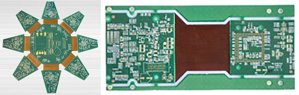
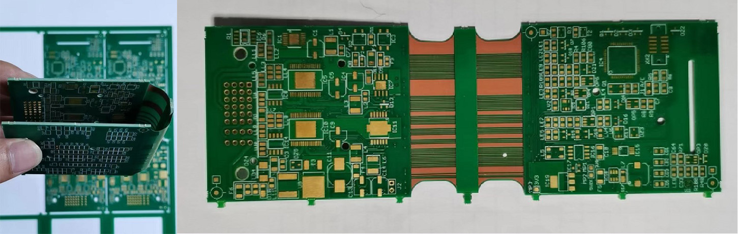
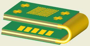
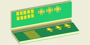
Rigid-Flex Board
More Efficient Advanced Technology & Perfect Solution.
Advantages of Rigid-Flex Board
Nowadays, design is increasingly pursuing miniaturization, low cost and high speed of products, especially in the mobile device market , which usually involves high-density electronic circuits. Using Rigid-Flex Boards will be an excellent choice for the peripheral devices connected through IO. Seven major advantages brought by the design requirements of integrating flexible board materials and rigid board materials in the manufacturing process, combining the 2 substrate materials with prepreg, and then achieving interlayer electrical connection of conductors through through-holes or blind/buried vias are as below:

3D assembly to reduce circuits
Better connection reliability
Reduce the number of components and parts
Better impedance consistency
Can design highly complex stacking structure
Implement a more streamlined appearance design
Reduce size
A rigid-flex is a board that combines rigidity and flexibility, processing both the rigidity of rigid board and flexibility of flexible board.
Semi FPC
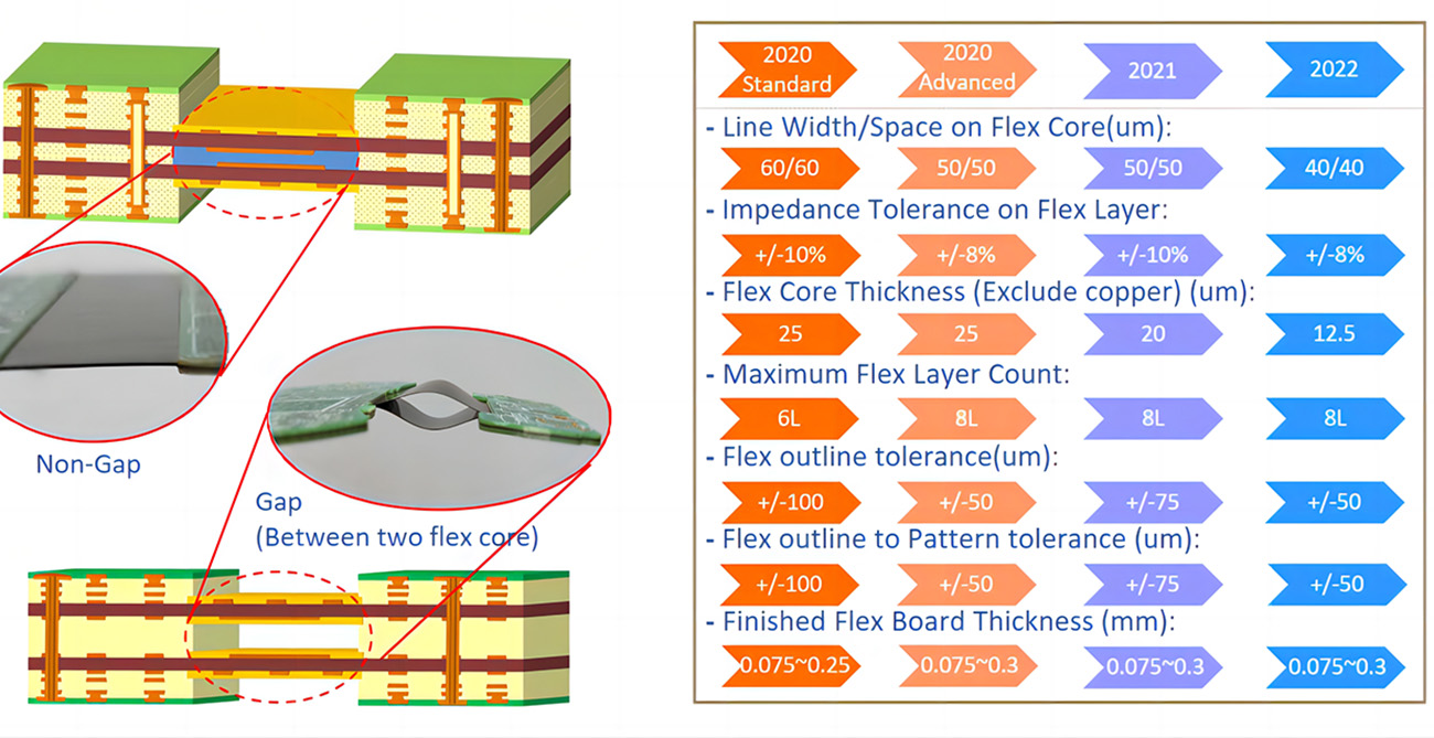
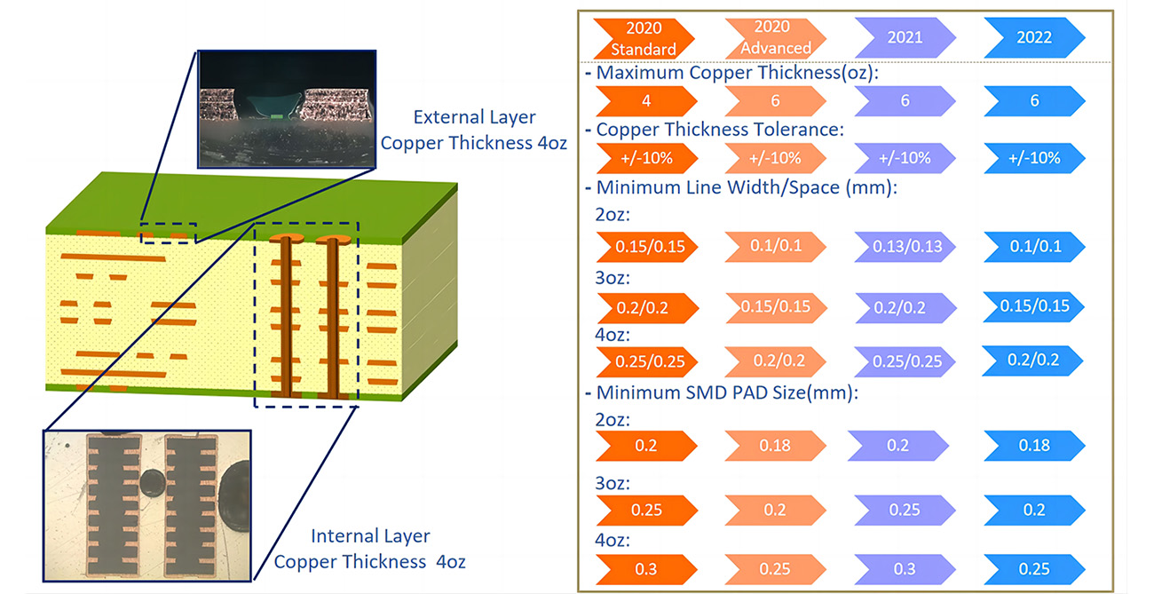
Capability Roadmap
| Item | Flex ‐ Rigid | Regal | Semi‐Flex |
| Figure | 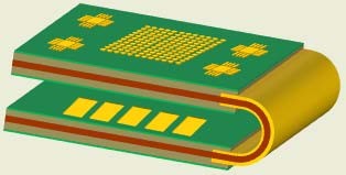 |
 |
 |
| Flexible Material | Polyimide | FR4 + Coverlay(Polyimide) | FR4 |
| Flexible thickness | 0.025~0.1mm(Exclude copper) | 0.05~0.1mm (Exclude copper) | Remained Thickness: 0.25+/‐0.05mm(Dedicated Material: EM825(I)) |
| Bending angle | Max 180° | Max 180° | Max 180°(Flex layer≤2) Max 90°(Flex layer>2) |
| Flexural Endurance;IPC‐TM‐650,Method 2.4.3. | <1000 cycle | < 25 cycle | NA |
| Bending Test; 1) Mandrel diam:6.25mm | <10K cycle(Bending Angle:180°) | <500 cycle(Bending Angle:180°) | <10 cycle(Bending Angle:180°) |
| Application | Flex to install & Dynamic(Single side) | Flex to install | Flex to install |
| Surface Finish | Typical Value | Supplier | |
| OSP |  |
0.2~0.6um;0.2~0.35um | Enthone Shikoku chemical |
| ENIG | 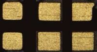 |
Au:0.03~0.12um, Ni :2.5~5um | ATO tech/Chuang Zhi |
| Selective ENIG | 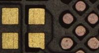 |
Au:0.03~0.12um, Ni :2.5~5um | ATO tech/Chuang Zhi |
| ENEPIG |  |
Au : 0.05~0.125um, Pd : 0.05~0.125um,Ni :5~10um | Chuang Zhi |
| Hard Gold |  |
Au:0.2~1.5um , Ni : min 2.5um | Platec |
| Soft Gold | 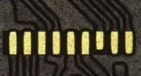 |
Au:0.15~0.5um , Ni : min 2.5um | EEJA |
| Immersion Tin |  |
Min: 1um | Enthone / ATO tech |
| Immersion Silver | 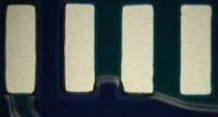 |
0.15~0.45um | Macdermid |
| HASL & Lead free HASL(OS) |  |
1~25um | Nihon Superior |
Au/Ni Type
● Gold plating can be divided into thin gold and thick gold according to thickness. Generally, gold below 4u”(0.41um) is called thin gold, while gold above 4u” is called thick gold. ENIG can only make thin gold, not thick gold. Only gold plating can make both thin and thick gold. The maximum thickness of thick gold on flexible board can be over 40u”. Thick gold is mainly used in working environments with bonding or wear resistance requirements.
● Gold plating can be divided into soft gold and hard gold by type. Soft gold is ordinary pure gold, while hard gold is cobalt containing gold. It’s precisely because cobalt is added that the hardness of the gold layer greatly increases exceeding 150HV to meet the wear resistance requirements.
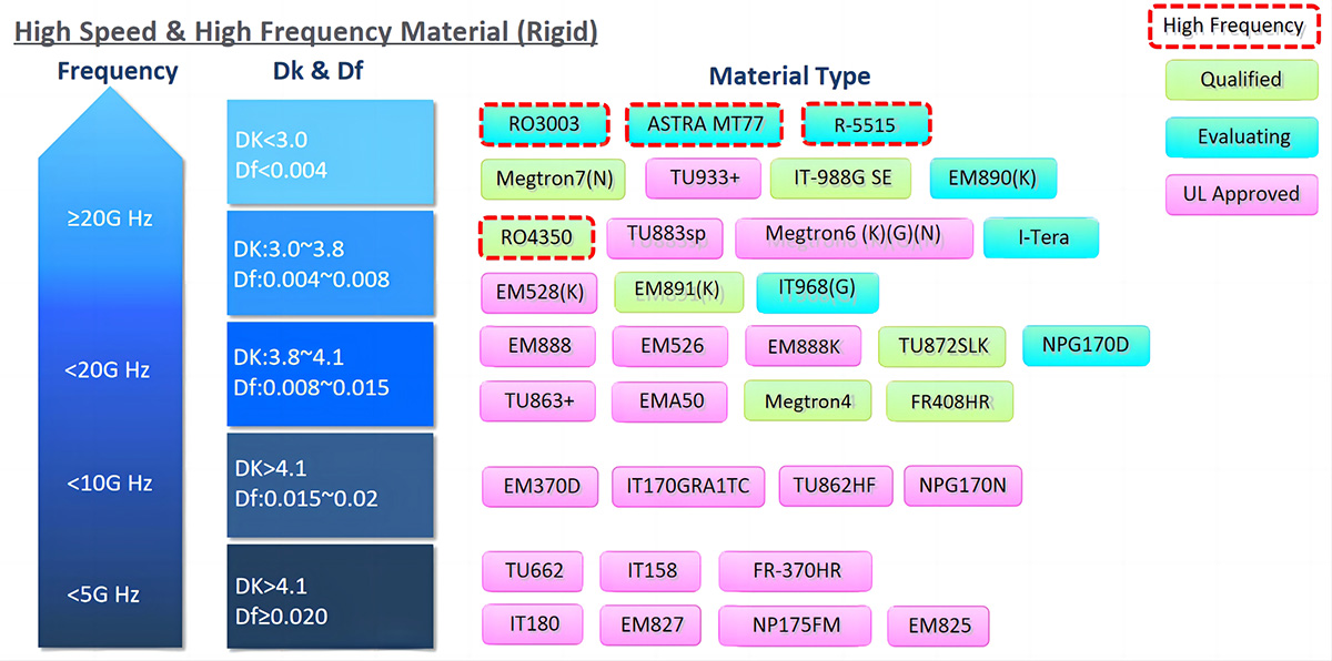
| Material Type | Properties | Supplier | |
| Rigid Material | Normal Loss | DK>4.2, DF>0.02 | NanYa / EMC / TUC / ITEQ / ShengYi / Isola / Doosan etc. |
| Middle Loss | DK>4.1, DF:0.015~0.02 | NanYa / EMC / TUC / ITEQ etc. | |
| Low Loss | DK:3.8~4.1, DF:0.008~0.015 | EMC / NanYa / TUC / Isola / Panasonic etc. | |
| Very Low Loss | DK:3.0~3.8, DF:0.004~0.008 | EMC / Panasonic / Rogers / TUC / Isola / ITEQ / NanYa etc. | |
| Ultra Low Loss | DK<3.0, DF<0.004 | Rogers / TUC / ITEQ / Panasonic / Isola etc. | |
| BT | Color:White / Black | MGC / Hitachi / NanYa / ShengYi etc. | |
| Copper Foil | Standard | Roughness(RZ)=6.34um | NanYa, KB, LCY |
| RTF | Roughness(RZ)=3.08um | NanYa, KB, LCY | |
| VLP | Roughness(RZ)=2.11um | MITSUI, Circuit Foil | |
| HVLP | Roughness(RZ)=1.74um | MITSUI, Circuit Foil | |
| Material Type | Normal DK/DF | Low DK/DF | |||
| Properties | Supplier | Properties | Supplier | ||
| Flex Material | FCCL(With ED & RA) | Normal Polyimide DK:3.0~3.3 DF:0.006~0.009 | Thinflex / Panasonic / Taiflex | Modified Polyimide DK:2.8~3.0 DF:0.003~0.007 | Thinflex / Taiflex |
| Coverlay(Black/Yellow) | Normal Adhesive DK:3.3~3.6 Df:0.01~0.018 | Taiflex / Dupont | Modified Adhesive DK:2.8~3.0 DF:0.003~0.006 | Taiflex / Arisawa | |
| Bond‐film(Thickness: 15/25/40 um) | Normal Epoxy DK:3.6~4.0 DF:0.06 | Taiflex / Dupont | Modified Epoxy DK:2.4~2.8 DF:0.003~0.005 | Taiflex / Arisawa | |
| S/M Ink | Solder mask;Color: Green / Blue / Black / White / Yellow / Red | Normal Epoxy DK:4.1 DF:0.031 | Taiyo / OTC / AMC | Modified Epoxy DK:3.2 DF:0.014 | Taiyo |
| Legend ink | Screen Color: Black / White / Yellow Inkjet Color: White | AMC | |||
| Other Materials | IMS | Insulated Metallic Substrates ( with Al or Cu ) | EMC / Ventec | ||
| High Thermal Conductive | 1.0 / 1.6 / 2.2 (W/M*K) | ShengYi / Ventec | |||
| EMI | Silver foil (SF‐PC6000‐U1 / SF‐PC8600‐C) | Tatsuta | |||
High Speed & High Frequency Material (Flexible)
| DK | Df | Material Type | |
| FCCL (Polyimide) | 3.0~3.3 | 0.006~0.009 | Panasonic R‐775 series;Thinflex A series;Thinflex W series;Taiflex 2up series |
| FCCL (Polyimide) | 2.8~3.0 | 0.003~0.007 | Thinflex LK series;Taiflex 2FPK series |
| FCCL (LCP) | 2.8~3.0 | 0.002 | Thinflex LC series;Panasonic R‐705T se;Taiflex 2CPK series |
| Coverlay | 3.3~3.6 | 0.01~0.018 | Dupont FR series; Taiflex FGA series; Taiflex FHB series;Taiflex FHK series |
| Coverlay | 2.8~3.0 | 0.003~0.006 | Arisawa C23 series;Taiflex FXU series |
| Bonding Sheet | 3.6~4.0 | 0.06 | Taiflex BT series;Dupont FR series |
| Bonding Sheet | 2.4~2.8 | 0.003~0.005 | Arisawa A23F series;Taiflex BHF series |
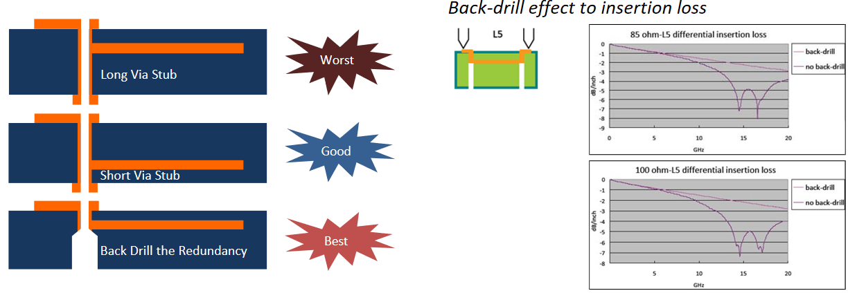
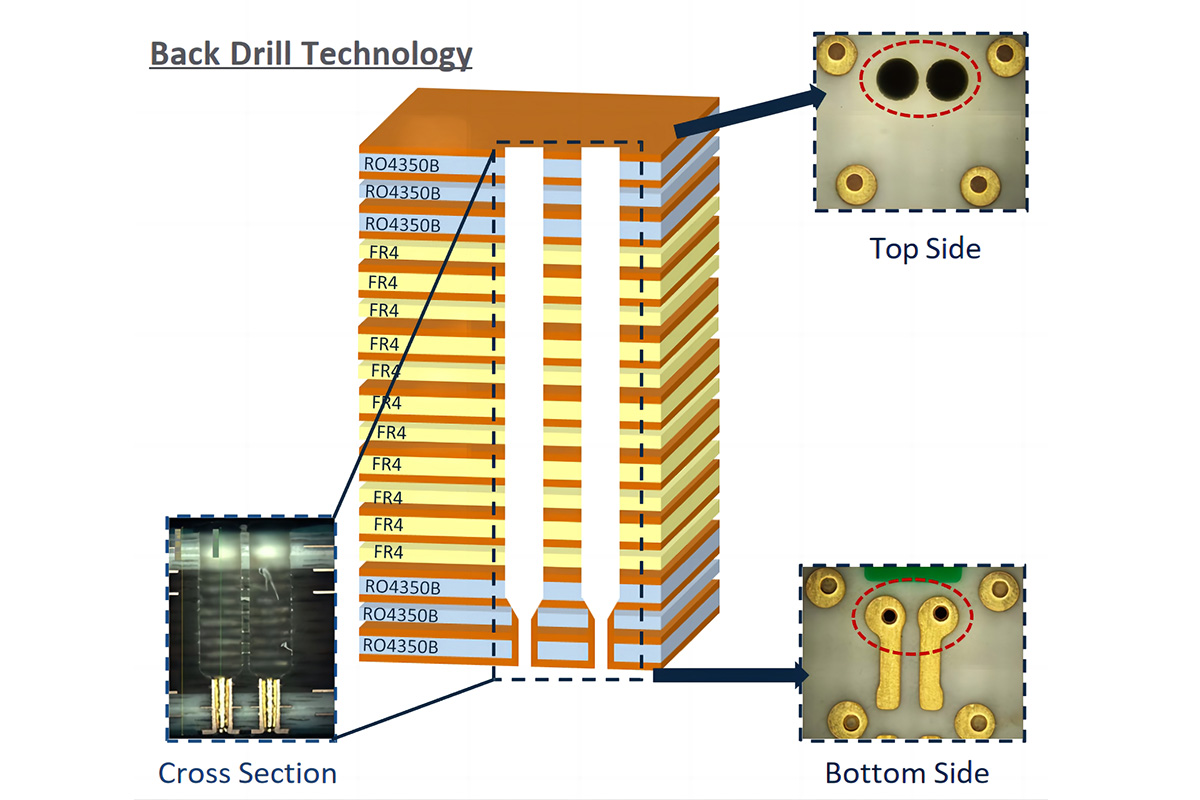
Back Drill Technology
● Microstrip traces should have no vias, they must be probed from the trace side.
● Trace on the secondary side should be probed from the secondary side(The launch side should be on that side).
● The good design is that stripline traces should be probed from whichever side most reduces the via stub.
● The best results for stripline will be obtained by using short vias that are backdrilled.
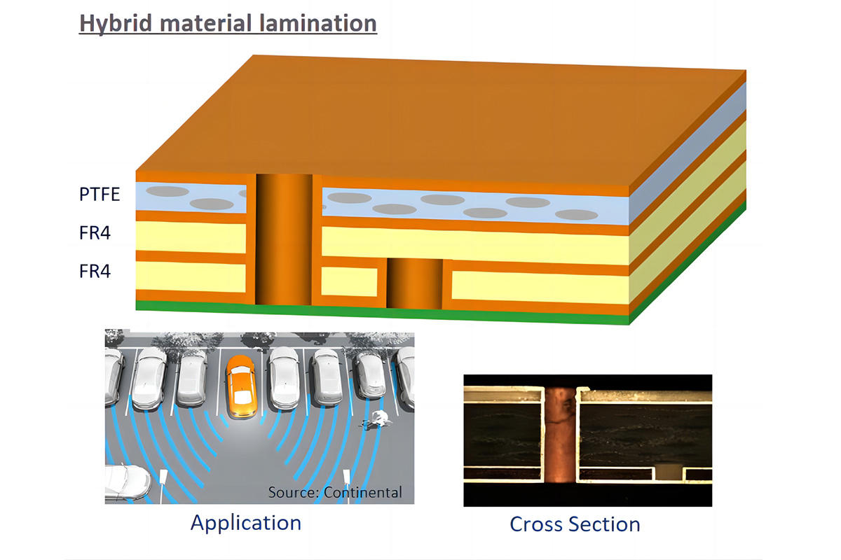
Product Application: Automotive radar sensor
Product Details:
4 Layer PCB with hybrid material (Hydrocarbon + Standard FR4)
Stack up: 4L HDI / Asymmetric
Challenge:
High frequency material with Standard FR4 Lamination
Controlled depth drill
Product Application: Automotive radar sensor
Product Details:
4 Layer PCB with hybrid material (Hydrocarbon + Standard FR4)
Stack up: 4L HDI / Asymmetric
Challenge:
High frequency material with Standard FR4 Lamination
Controlled depth drill
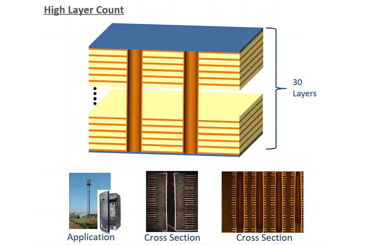
Product Application:
Base station
Product Details:
30 Layers (Homogeneous material)
Stack up: High layer count / Symmetric
Challenge:
Registration for each layers
High aspect ratio of PTH
Critical lamination parameter
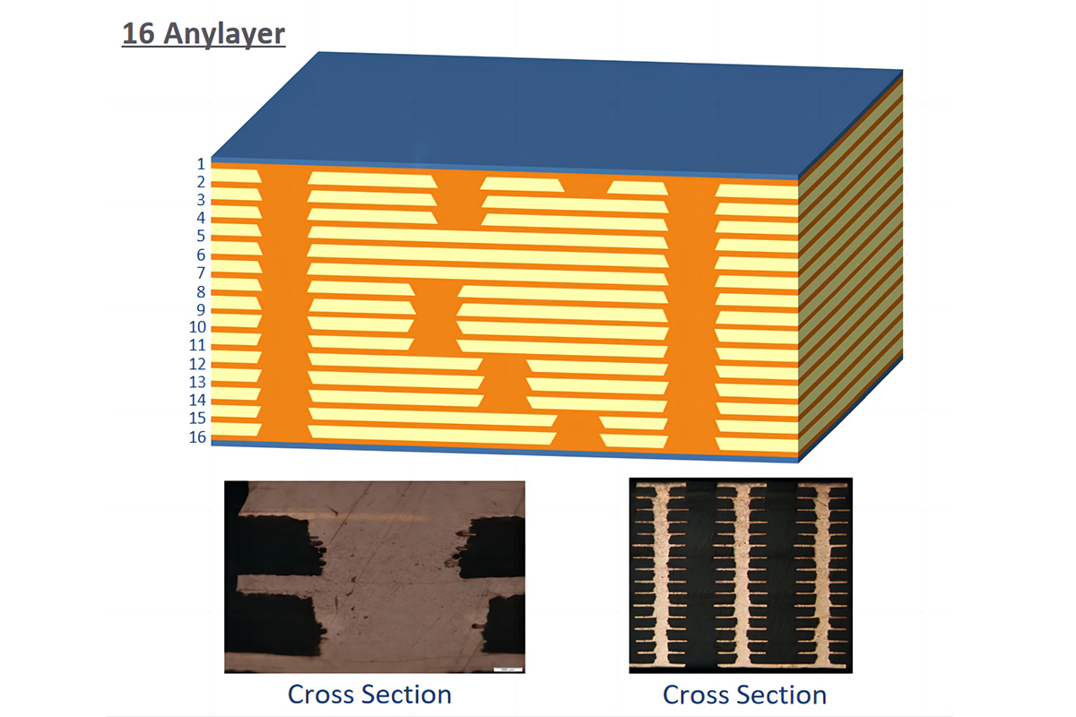
Product Application:
Memory
Product Details:
Stack up: 16 Layers Anylayer
IST Test: Condition:25‐190℃ Time:3 min, 190‐25℃ Time:2min, 1500 Cycles. Resistance change rate≤10%, Test method:IPC‐TM650‐2.6.26. Result: Pass.
Challenge:
Laminating more than 6 times
Laser vias accuracy
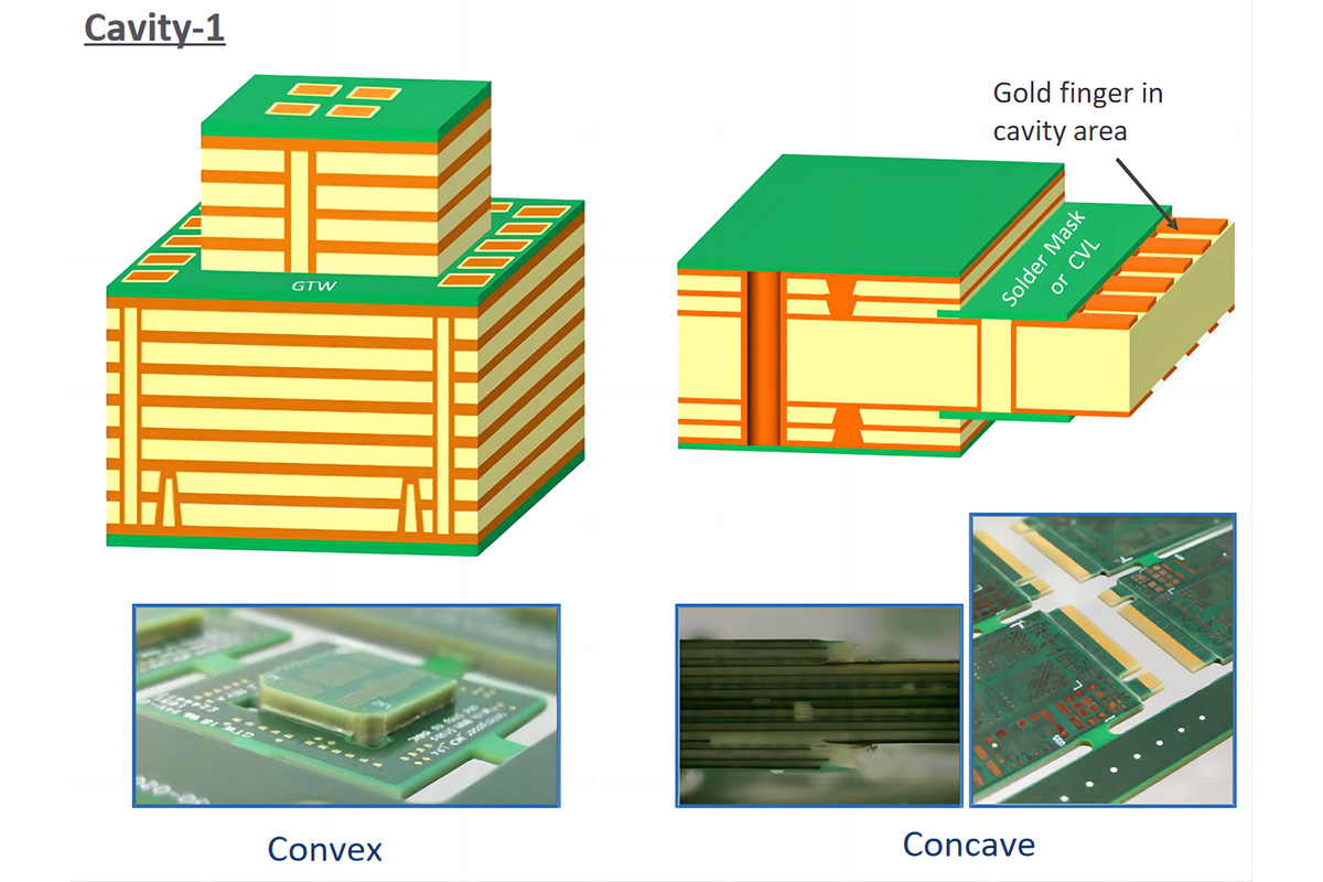
Product Application:
Memory
Product Details:
Stack up: Cavity
Material: Standard FR4
Challenge:
Using De‐cap technology on Rigid PCB
Registration between layers
Less squeeze out at the step area
Critical beveling process for the G/F
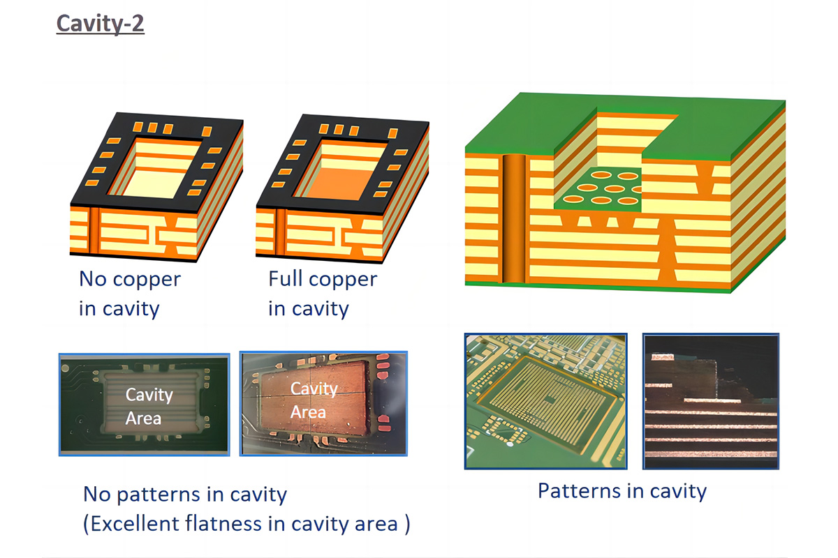
Product Application:
Camera Module / Notebook
Product Details:
Stack up: Cavity
Material: Standard FR4
Challenge:
Using De‐cap technology on Rigid PCB
Critical laser program and parameters in De‐cap process
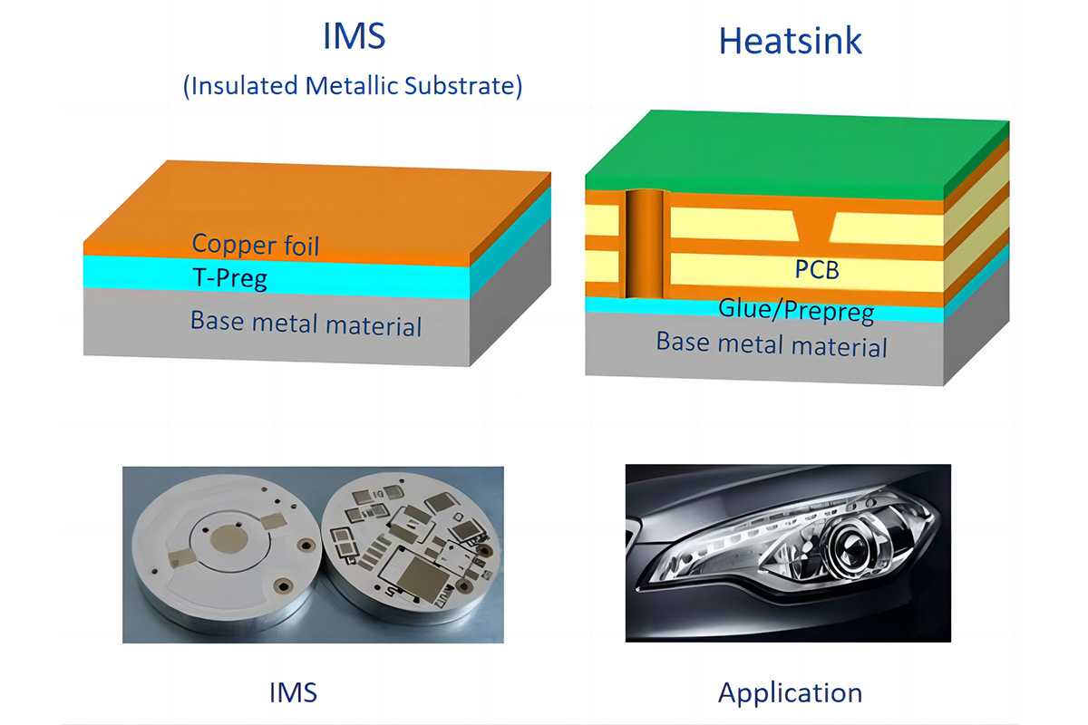
Product Application:
Automotive lamps
Product Details:
Stack up: IMS / Heatsink
Material: Metal + Glue/Prepreg + PCB
Challenge:
Aluminum base and copper base (single layer)
Thermal conductivity
FR4+ Glue/Prepreg + Al lamination
Advantages:
Great Heat Dissipation
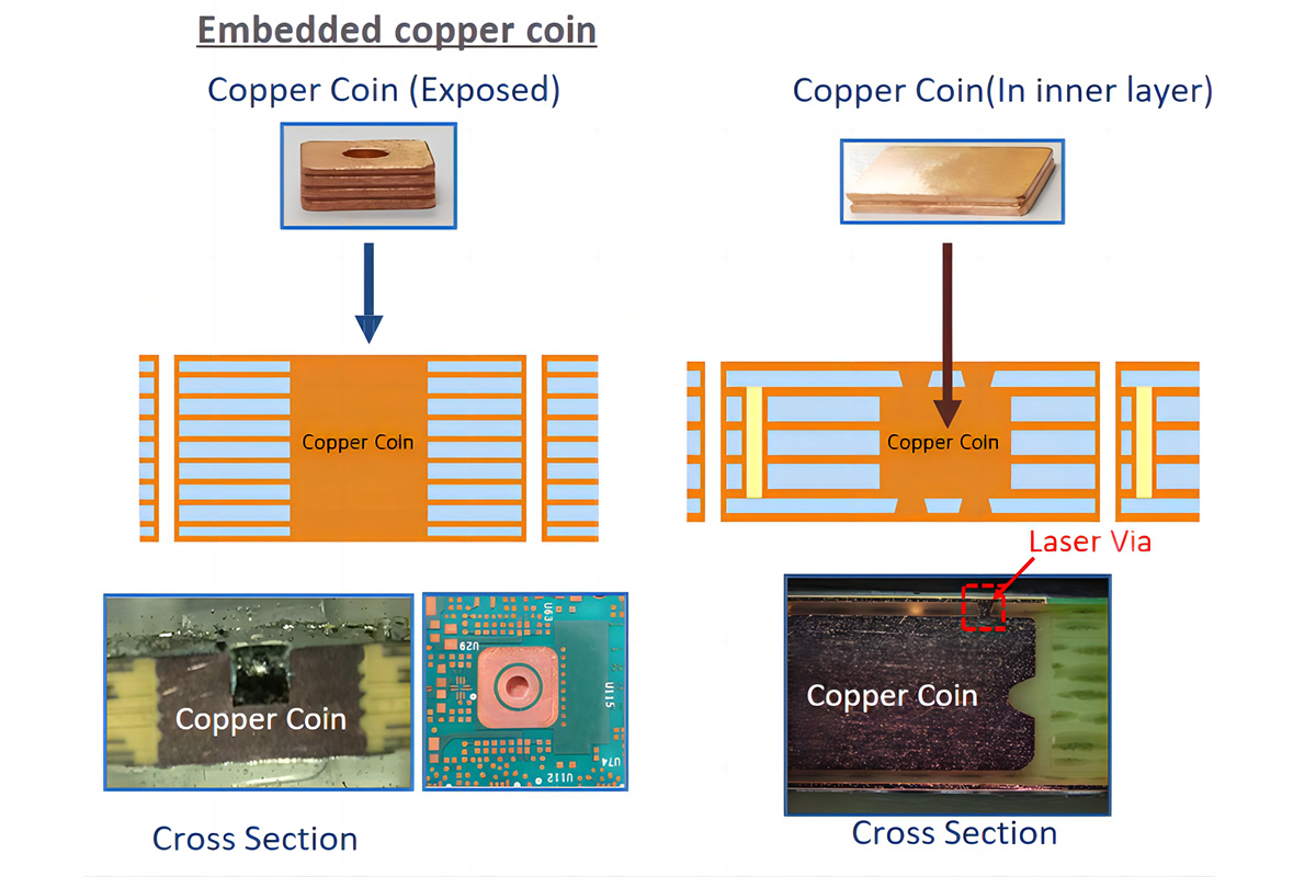
Product Details:
High speed material (Homogeneous)
Stack up: Embedded copper coin / Symmetric
Challenge:
Accuracy of coin dimension
Accuracy of lamination opening
Critical resin flow
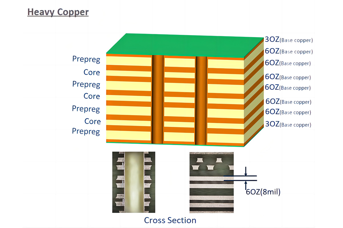
Product Application:
Automotive / Industrial / Base station
Product Details:
Internal layer base copper 6OZ
External layer base copper 3OZ/6OZ Stack up:
6OZ copper weight in internal layer
Challenge:
6OZ copper gap filled fullly with epoxy
No drift in lamination processing
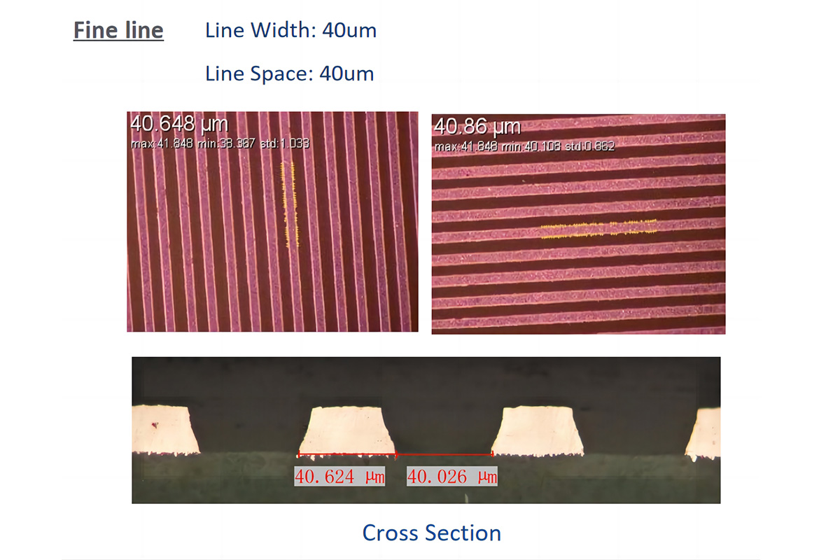
Product Application:
Smart phone / SD Card / SSD
Product Details:
Stack up: HDI / Anylayer
Material: Standard FR4
Challenge:
Very low profile/RTF Cu foil
Plating uniformity
High resolution dry film
LDI Exposure (Laser Direct Image)
Product Application:
Communication / SD Card / Optical Module
Product Details:
Stack up: HDI / Anylayer
Material: Standard FR4
Challenge:
None gap at the finger edge when PCB in the plating gold processing
Special resistant film
Product Application:
Industrial
Product Details:
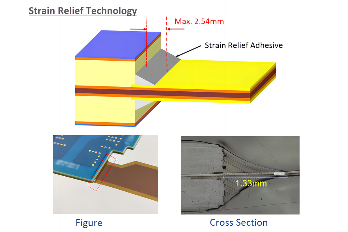
Stack up: Rigid‐Flex
With Eccobond at Rigid‐Flex transformation
Challenge:
Critical moving speed and depth for shaft
Critical air pressure parameter