
Leave Your Message
-
E-mail
-
Whatsapp
-
Message
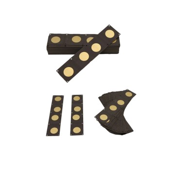
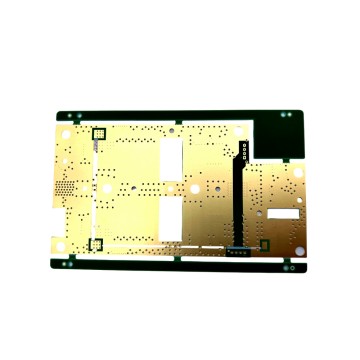
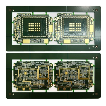
Explore our flagship PCB products engineered for high-frequency, high-reliability autonomous driving sensor applications.
A Watch PCB — compact, ultra-thin, and precision-manufactured — represents one of the most demanding categories in modern printed circuit board engineering. Originally developed for miniaturized wearable electronics, Watch PCB technology has evolved far beyond consumer devices. Today, its core attributes — extreme miniaturization, multi-layer stack-up, high-frequency signal integrity, and thermal stability — make it a critical enabling technology for autonomous driving sensor systems.
Autonomous vehicles rely on a complex ecosystem of sensors: millimeter-wave radar, LiDAR, ultrasonic sensors, high-resolution cameras, and inertial measurement units (IMUs). Each of these sensors requires a dedicated PCB that can process signals at high speed, resist electromagnetic interference, maintain dimensional stability across extreme temperature ranges, and fit within tightly constrained form factors. This is precisely where Watch PCB engineering principles deliver transformative value.
The convergence of Watch PCB miniaturization technology with the stringent reliability demands of automotive-grade electronics is reshaping how sensor modules are designed, manufactured, and validated. As autonomous driving systems advance from Level 2 to Level 4 and Level 5 autonomy, the PCBs at the heart of every sensor node must keep pace — delivering higher performance in smaller packages, with zero tolerance for failure.
Watch PCBs leverage low-loss dielectric materials (Rogers, Taconic, PTFE) to support signal frequencies up to 77 GHz and beyond — essential for millimeter-wave radar sensors used in adaptive cruise control and collision avoidance systems.
High-Density Interconnect (HDI) technology with micro-via, buried via, and blind via structures enables Watch PCBs to pack more functionality into sensor modules smaller than a matchbox — critical for in-wheel and bumper-integrated sensor designs.
With TG170 and above glass transition temperatures, Watch PCBs for autonomous driving sensors maintain structural and electrical integrity from -40°C to +150°C, meeting IATF 16949 and AEC-Q100 automotive reliability standards.
Precision impedance control (±5% tolerance) across all signal layers ensures that high-speed data from camera ISPs, LiDAR point-cloud processors, and radar DSPs arrives without reflections, jitter, or crosstalk — preserving sensor accuracy.
Hybrid PCB stack-ups with embedded shielding layers and selective metal edge treatments prevent electromagnetic interference between sensor channels — a mandatory requirement in multi-sensor autonomous driving platforms.
From bare board fabrication through SMT assembly, DIP, programming, and functional testing — integrated PCBA manufacturing reduces supply chain risk and accelerates sensor module time-to-market for automotive OEMs and Tier-1 suppliers.
The global autonomous driving market is projected to exceed $550 billion by 2030, with sensor hardware representing one of the largest cost and technology investment categories. Each autonomous vehicle platform — whether a robotaxi, a highway pilot passenger car, or a last-mile delivery robot — integrates between 10 and 40 discrete sensor modules. Every one of these modules contains one or more precision PCBs. The cumulative demand for automotive-grade, high-frequency PCBs is accelerating at a compound annual growth rate exceeding 18%.
Watch PCB manufacturers have emerged as strategic suppliers to this ecosystem. Their mastery of compact, multi-layer, high-frequency board design positions them uniquely to serve sensor module manufacturers who require both miniaturization and reliability. Major automotive Tier-1 suppliers including Bosch, Continental, Aptiv, and Valeo have increasingly sourced specialized PCB substrates from high-technology manufacturers capable of meeting both automotive quality standards and advanced RF performance specifications.
Beyond passenger vehicles, Watch PCB technology for autonomous driving sensors finds critical application across a broad industrial spectrum. In autonomous trucking, long-range radar sensors mounted on front fascias require PCBs that can withstand highway vibration, temperature cycling, and moisture ingress while maintaining 77 GHz signal performance over a service life exceeding 15 years. In autonomous mobile robots (AMRs) used in logistics warehouses, compact 2D/3D LiDAR sensor PCBs must operate continuously in environments ranging from freezer storage to high-temperature loading docks.
Agricultural autonomous machinery represents another high-growth application: GPS-guided tractors and harvesters integrate multi-sensor fusion systems requiring PCBs with exceptional resistance to dust, humidity, and mechanical shock. In smart infrastructure — including roadside perception units and intelligent traffic management nodes — Watch PCB-based sensor boards process real-time vehicle detection data 24/7, demanding both ultra-reliability and cost efficiency at scale.
The defense and military sector represents perhaps the most demanding application domain. Unmanned ground vehicles (UGVs) and autonomous reconnaissance drones require sensor PCBs qualified to MIL-SPEC standards, combining the miniaturization of Watch PCB technology with military-grade environmental protection and EMI hardening.
Next-generation 4D imaging radar systems — capable of resolving velocity, azimuth, elevation, and range simultaneously — demand PCBs with antenna-in-package (AiP) integration at frequencies approaching 300 GHz. Watch PCB manufacturers are developing ultra-low-loss substrates and sub-100-micron trace geometries to enable this leap in radar resolution.
As sensor fusion AI moves from central compute units to edge processing within individual sensor modules, Watch PCBs must accommodate high-power AI SoCs alongside RF front-ends. This demands advanced thermal management layers, embedded copper coin heat dissipation, and co-designed power delivery networks — all within a board footprint measured in square centimeters.
Automotive Ethernet (100BASE-T1, 1000BASE-T1) and Time-Sensitive Networking (TSN) protocols are replacing legacy CAN bus in autonomous platforms. Watch PCBs for sensor modules must now support multi-gigabit differential pair routing with precise impedance matching and minimal skew — a significant advancement over traditional automotive PCB design rules.
Regulatory pressure from RoHS, REACH, and emerging EU End-of-Life Vehicle directives is driving the transition to halogen-free, low-CTE laminate systems for automotive PCBs. Advanced Watch PCB manufacturers are qualifying next-generation eco-friendly high-frequency materials that meet both environmental standards and demanding RF performance requirements.
The shift towards software-defined vehicles means sensor hardware — including PCBs — must support over-the-air (OTA) firmware updates, in-field reconfiguration, and modular hardware refresh cycles. Watch PCBs are being designed with programmable logic integration and standardized connector interfaces to support this flexible deployment model.
To further reduce sensor module size and improve signal integrity, Watch PCB technology is advancing towards embedded resistors, capacitors, and inductors within the PCB substrate itself — eliminating surface-mount components and reducing parasitic inductance in high-frequency sensor signal chains by up to 60%.
Automotive radar operating at 76–81 GHz is the backbone of autonomous driving perception — enabling adaptive cruise control, emergency braking, blind-spot monitoring, and pedestrian detection in all weather conditions. The PCB substrate for a radar front-end module must exhibit an extremely low dielectric loss tangent (Df ≤ 0.002) and tightly controlled dielectric constant (Dk = 3.0 ± 0.05) to ensure antenna gain and beam-steering accuracy. Watch PCB technology — with its mastery of PTFE-based and ceramic-filled high-frequency laminates — is ideally positioned to manufacture these ultra-precision RF substrates. Hybrid pressing techniques combine high-frequency antenna layers with standard FR4 digital processing layers in a single compact board, reducing module size by up to 35% compared to conventional two-board designs.
High-resolution automotive cameras — capturing 8MP to 12MP images at 60 fps — generate data rates exceeding 4 Gbps per channel. The image signal processor (ISP) PCB must route these ultra-high-speed differential pairs with sub-5-mil impedance tolerance while managing the substantial thermal output of advanced vision SoCs. Watch PCB HDI technology, with its fine-pitch micro-via structures and embedded thermal management layers, enables camera module PCBs that are both thermally efficient and electromagnetically clean — preventing ISP noise from contaminating adjacent radar or LiDAR sensor channels in tightly packaged sensor clusters.
Solid-state and MEMS-based LiDAR systems require PCBs that simultaneously handle high-voltage laser driver circuits (operating at 20–100V), low-noise avalanche photodiode (APD) receiver front-ends, and high-speed time-of-flight (ToF) measurement ASICs. The co-existence of these disparate circuit domains on a single compact PCB demands sophisticated power plane isolation, guard ring structures, and controlled impedance routing — all hallmarks of advanced Watch PCB design methodology. Richpcba's high-frequency hybrid pressing technology enables the integration of these mixed-signal domains within a single compact board, reducing interconnect latency and improving LiDAR point-cloud update rates.
Parking assistance and low-speed maneuvering systems deploy arrays of 8–12 ultrasonic sensors distributed around the vehicle perimeter. Each sensor node contains a compact PCB managing transducer drive, echo reception, and CAN/LIN communication. The miniaturization demands of bumper-integrated ultrasonic sensor housings — with PCB footprints as small as 20mm × 15mm — align perfectly with Watch PCB manufacturing capabilities, including fine-pitch SMT assembly, selective conformal coating, and automated optical inspection (AOI) to 100% coverage.
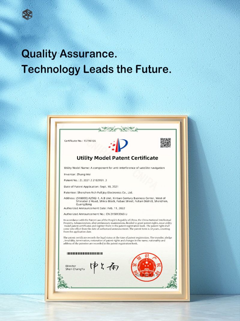
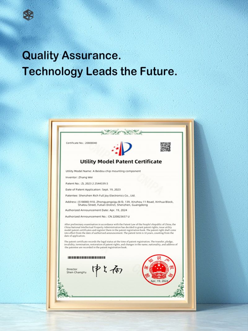
Inertial Measurement Units and GNSS receivers provide the dead-reckoning and absolute positioning backbone of autonomous navigation. These sensor PCBs must achieve exceptional vibration isolation, thermal compensation, and EMI immunity to deliver centimeter-level positioning accuracy. Watch PCB technology contributes through precision impedance-matched RF trace routing for GNSS antenna feeds, low-vibration via-in-pad construction, and Beidou/GPS dual-frequency antenna integration — capabilities directly supported by Richpcba's patented satellite navigation anti-interference component technology.
Your trusted partner for Watch PCB and high-frequency PCB solutions for autonomous driving sensor systems.

Based in China and looking at the global market, Shenzhen Rich Full Joy Electronics Co., Ltd. has been committed to industry development for 20 years. The company is a national high-tech innovative enterprise that combines focus and expertise. It's also an important enterprise incubation base in China. We specialize in providing customers with one-stop intelligent electronic manufacturing services, including scientific research, PCB design, PCB manufacturing, PCB assembly (including SMT, DIP, Programming and testing) and component selection.
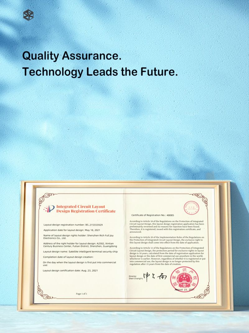
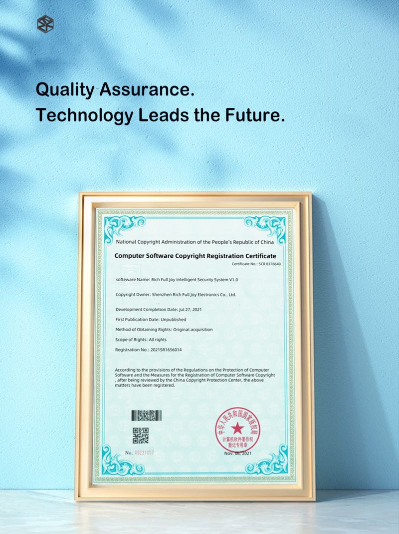
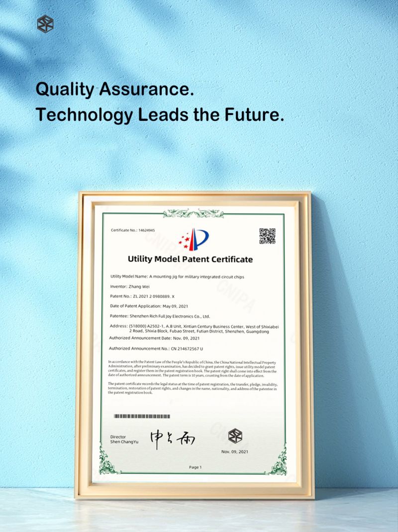
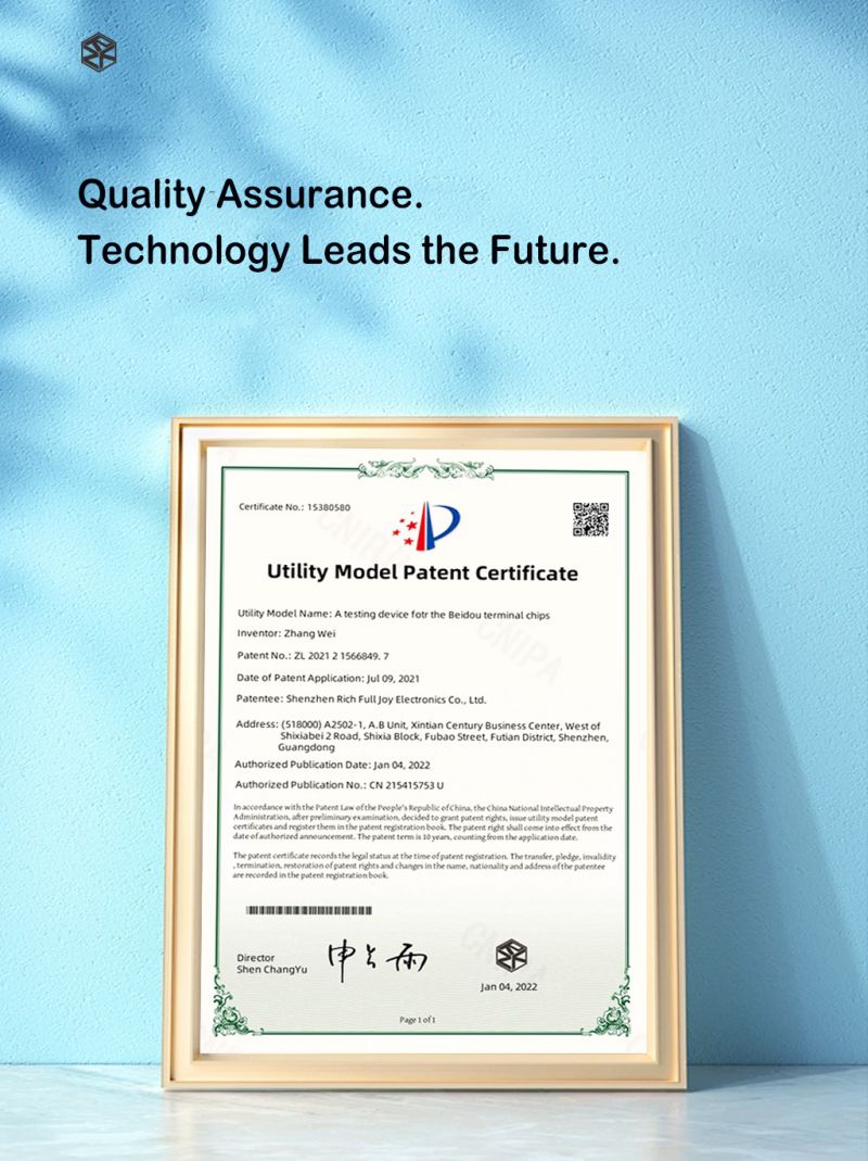
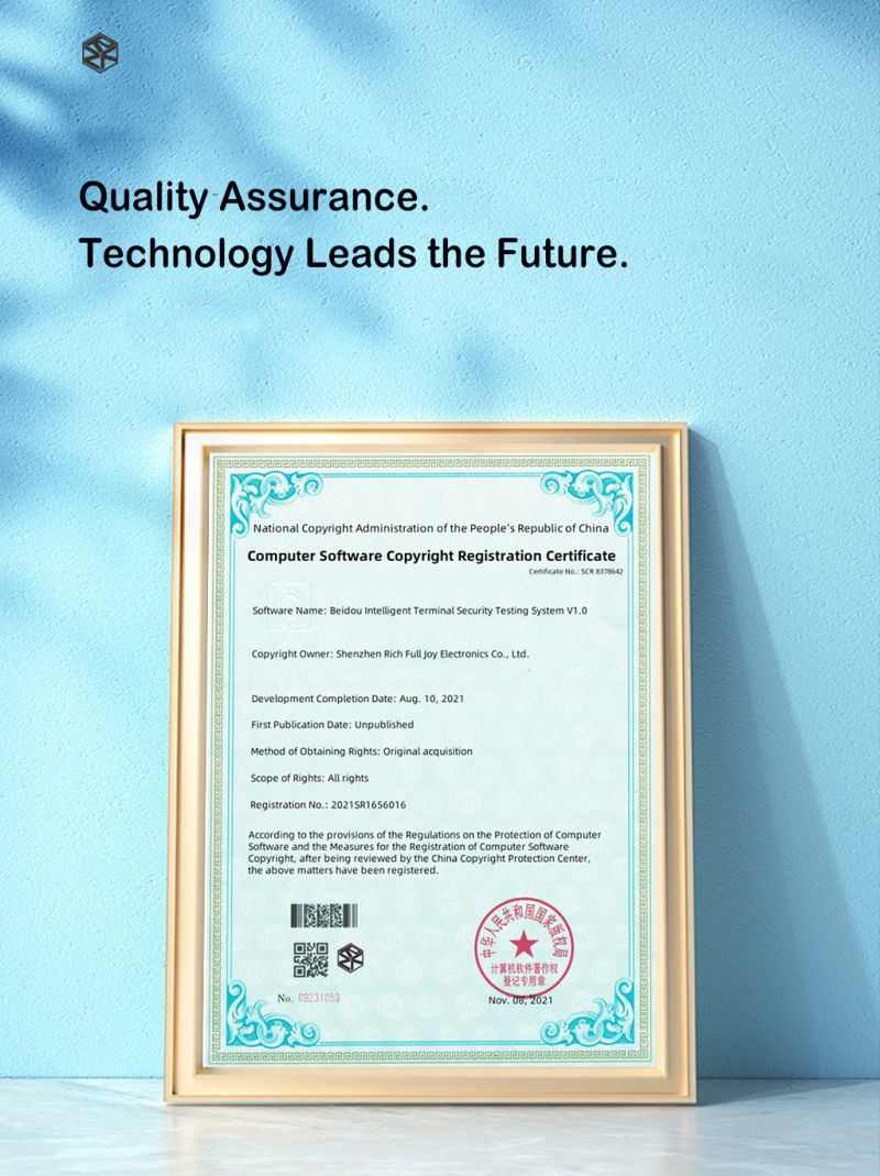
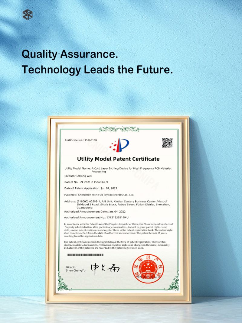
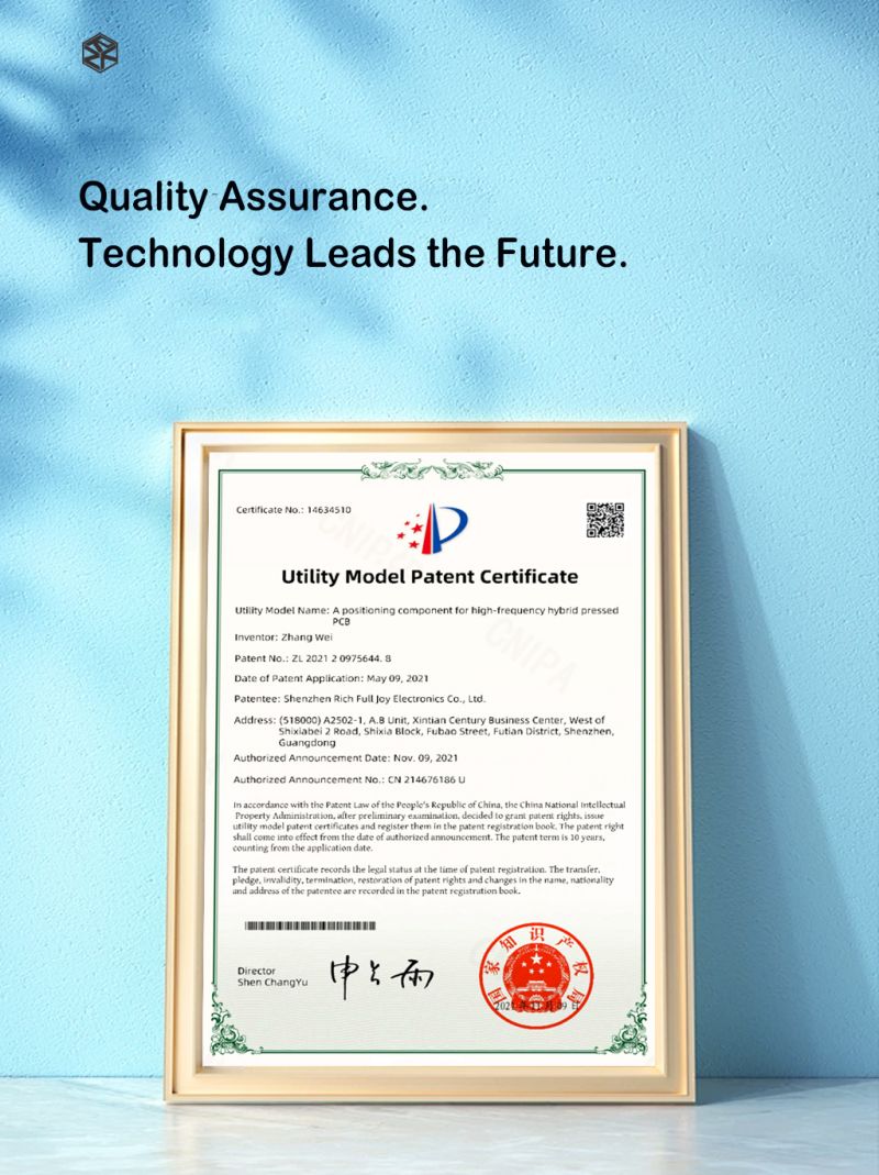
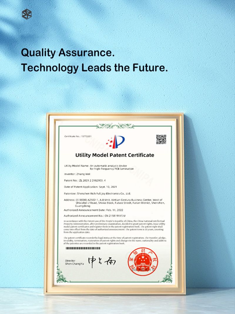
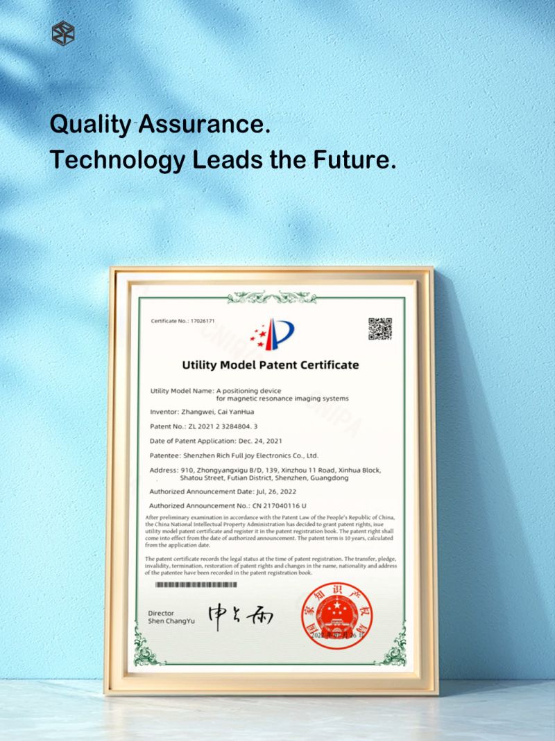
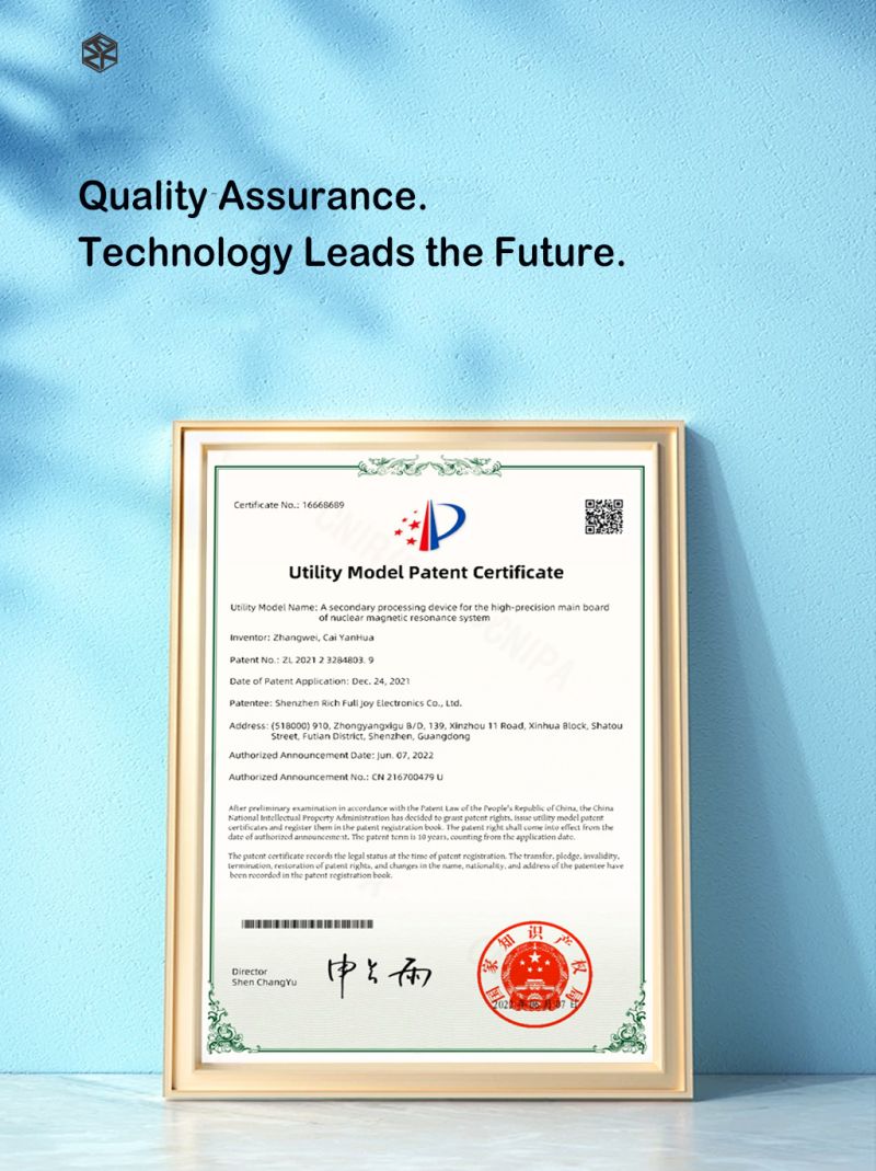
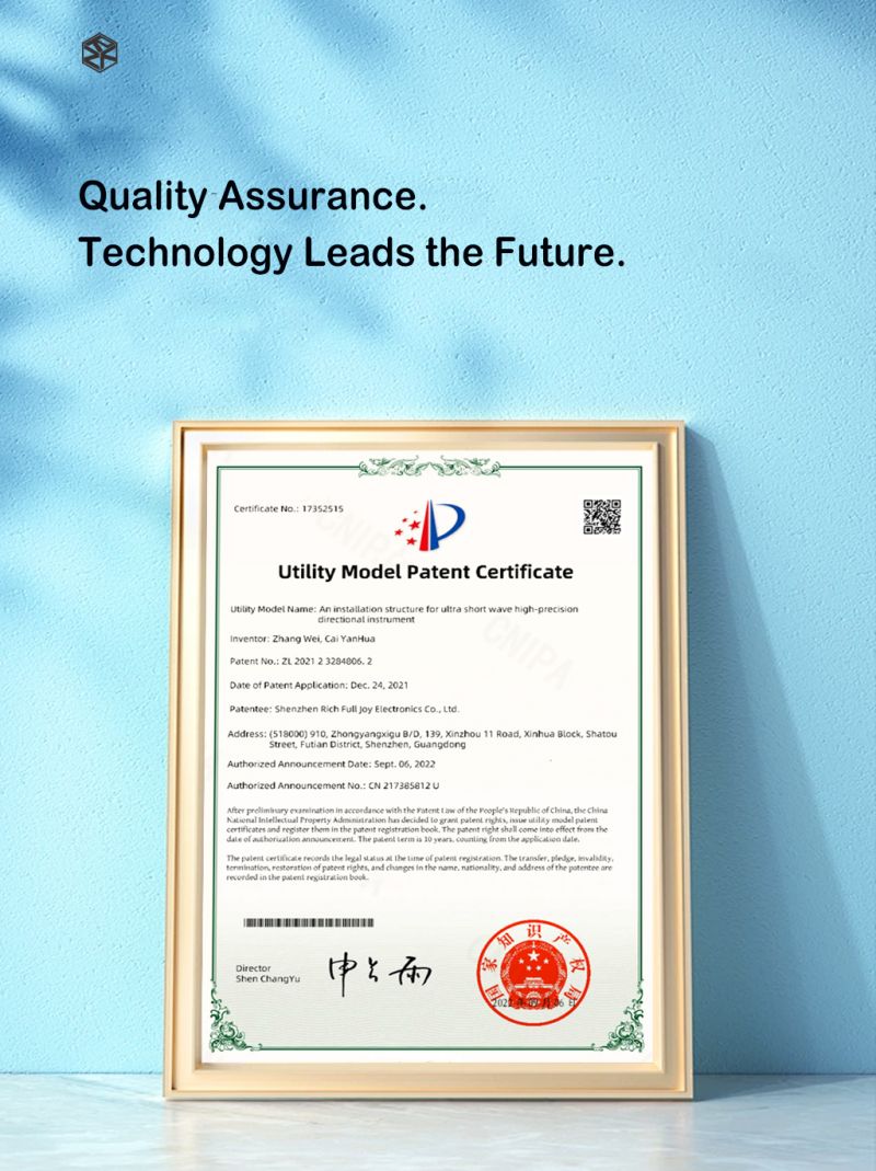
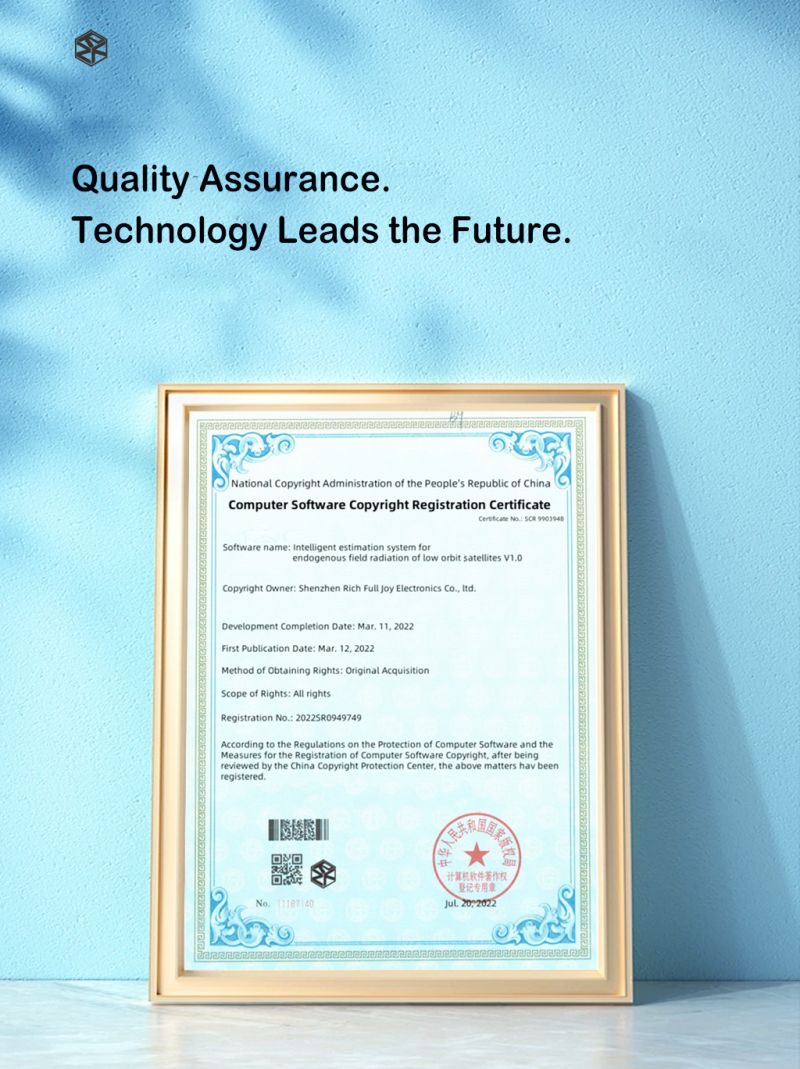
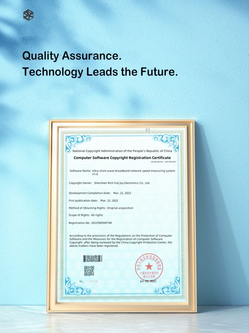
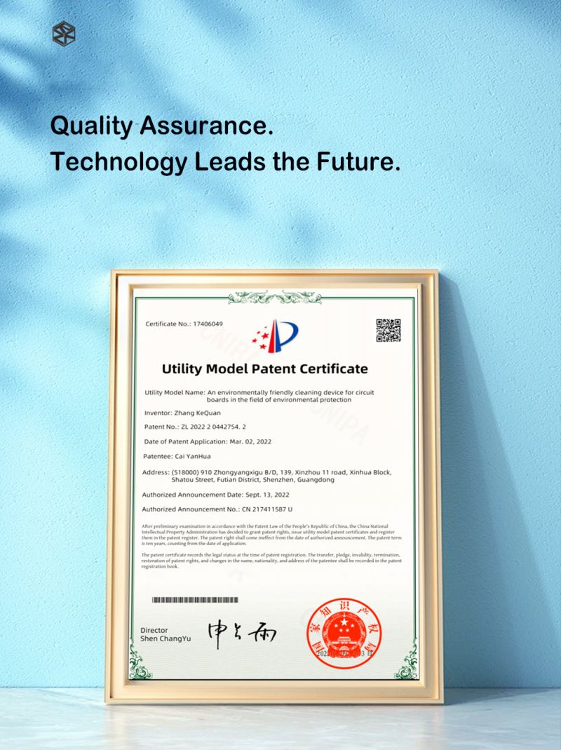
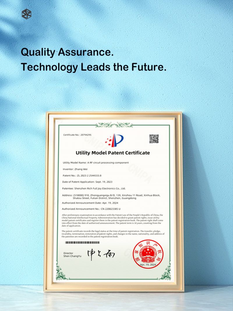
Technological innovation is the core competitiveness of our enterprise. We've obtained multiple invention and utility model patents, and have passed various international standard certifications such as ISO9001, IATF16949, ISO14001, UL, CQC, REACH, RoHS, COC, as well as the GJB9001C-2017 standard certification for weapon and equipment quality management system.
We've provided high-quality and reliable products to multiple research institutions, universities, and assisted customers in identifying design issues and providing reasonable suggestions and processing parameters. We not only publish technical papers, but also actively participate in domestic and overseas technology exchange conferences to spread academic value and cutting-edge technological innovation. We regularly communicate with customers and strive to provide them with the best solutions.
Our extensive portfolio of patents and certifications reflects our commitment to innovation and quality in every Watch PCB we manufacture for autonomous driving sensor applications.





Discover our full range of high-frequency, high-reliability PCB solutions designed for every layer of the autonomous driving sensor stack.
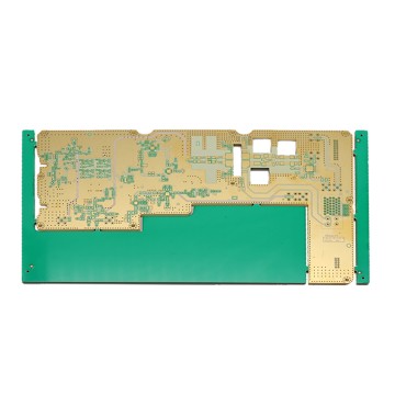
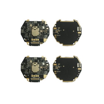

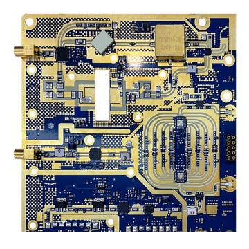

Contact Shenzhen Rich Full Joy Electronics today to discuss your Watch PCB requirements for autonomous driving sensor applications. From rapid prototyping to high-volume production, our engineering team is ready to deliver solutions that meet your exact specifications.
Get a Custom PCB Quote →