


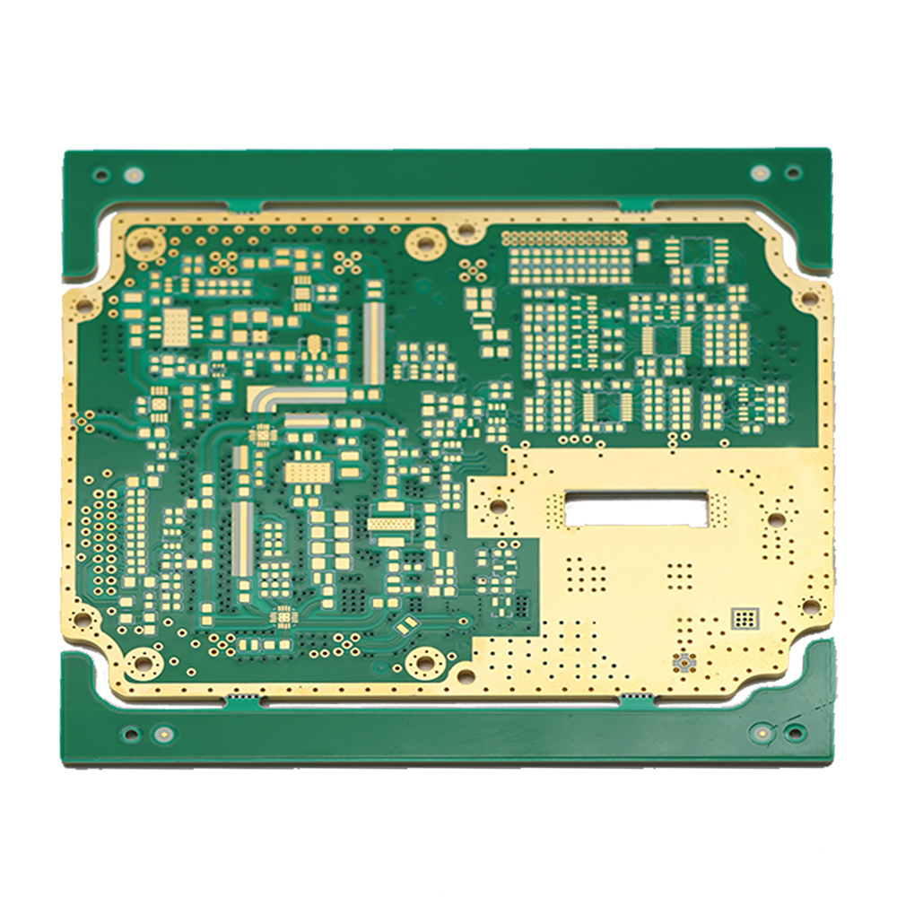


16L Any Layer HDI PCB , IC Test Board


Product manufacturing instructions
| Type | Any layer HDI impedance resin plug hole step groove |
| Materia | High-speed Series EM370D |
| Number of layer | 16L |
| Board Thickness | 1.6mm |
| Single size | 70*91.89mm/1PCS |
| Surface finish | ENEPIG |
| Inner copper thickness | 35um |
| Outer copper thickness | 35um |
| Color of solder mask | green(GTS,GBS) |
| Silkscreen color | white(GTO,GBO) |
| Via treatment | resin plug hole+microvia fi lling |
| Density of mechanical drilling hole | 19W/㎡ |
| Density of laser drilling hole | 100W/㎡ |
| Min via size | 0.1mm |
| Min line width/space | 2/2mil |
| Aperture ratio | 12mil |
| Pressing times | 6 time |
| Drilling times | 7time |
| PN | E1691047 |
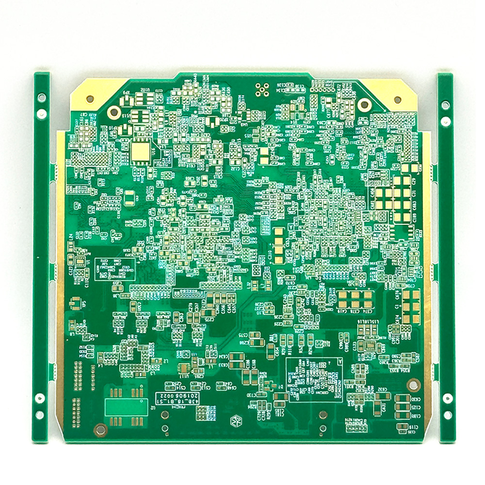
Understanding PCB Stacking Structure: A Comprehensive Guide

3. Insulation Layers
Insulation layers, commonly made from materials such as polyimide or FR-4, are positioned between the conductive layers. Their primary function is to provide electrical isolation, preventing short circuits and signal interference between layers. The quality of the insulation layers directly affects the PCB's electrical performance, especially in high-frequency or high-density applications.
4. Solder Mask Layer
The outermost layer of the PCB is the solder mask layer, typically green, which protects the board from solder short circuits and environmental damage. This layer enhances soldering quality by ensuring solder adheres only to the required pads, reducing the risk of soldering defects like cold solder joints and solder bridges.
5. Silkscreen Layer
In addition to the primary layers, many PCBs include a silkscreen layer. This layer is used for printing component labels, numbers, and other essential information on the board. It aids in proper component placement during assembly and provides valuable reference for maintenance and repair.
SEO Keywords: PCB stacking structure, PCB substrate layer, PCB conductive layers, PCB insulation layers, PCB solder mask layer, PCB silkscreen layer, Printed Circuit Board design
By understanding and optimizing the PCB stacking structure, manufacturers can achieve complex electrical connections and ensure high performance and longevity of electronic products. Each layer within the stacking structure plays a critical role in the PCB's functionality, ensuring reliable operation in various working environments.
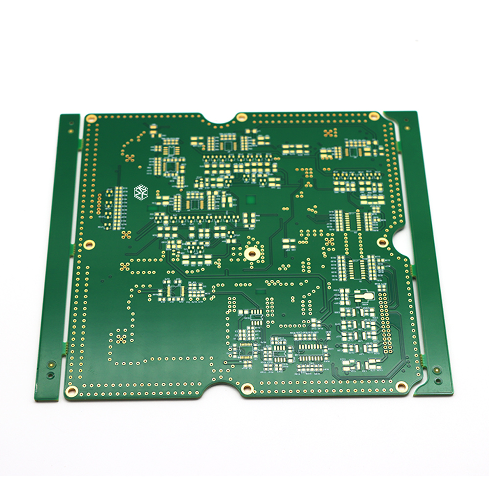
PCB Cross-Section Inspection Project: Comprehensive Understanding and Defect Identification

Interlayer Connections: Examine the state of interlayer connections to check for poor connectivity or short circuits.
Line Width and Thickness: Measure the width and thickness of the lines to ensure they meet design specifications. Lines that are too wide or too thin can impact current conduction performance.
Hole Quality: Inspect the size and position of drilled holes, and ensure the walls are smooth and free from cracks. Hole issues can lead to poor electrical connections or insufficient mechanical strength.
Material Consistency: Assess the consistency of PCB materials, including the thickness and uniformity of insulation materials. Inconsistent materials can cause fluctuations in circuit board performance.
How to Identify Defective Products:
Through cross-section inspection, defective products can be identified based on the following characteristics:
Peeling or Delamination: Layer delamination usually indicates the use of substandard adhesives or process issues during production.
Copper Foil Peel-Off: Copper foil detachment may be due to improper temperature control or material quality issues during production.
Pad Damage: Pad damage is typically caused by improper handling or material defects during manufacturing.
Hole Issues: Inaccurate or defective holes can affect the functionality and reliability of the circuit board.
Through comprehensive cross-section inspection, we can promptly detect and correct these issues, ensuring the quality and reliability of PCB products to meet high customer standards. Accurate inspection not only enhances product performance but also reduces later repair and maintenance costs, providing customers with the highest quality circuit board solutions.
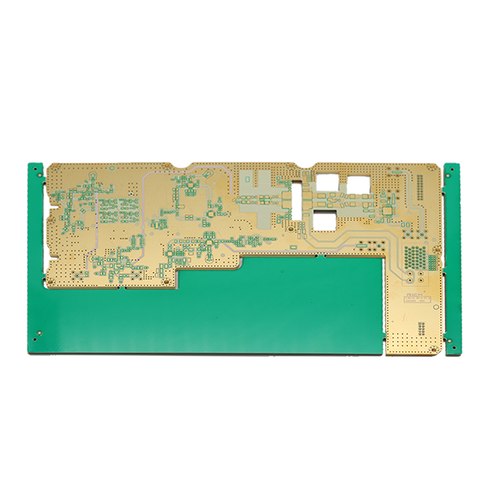
Applications of Arbitrary Interconnect PCBs

Medical Devices
In medical devices such as electrocardiogram (ECG) machines, ultrasound scanners, and monitors, arbitrary interconnect PCBs provide complex circuit connections to ensure high-precision measurements and data processing capabilities.
Automotive Electronics
Various electronic systems in modern vehicles, such as infotainment systems, navigation systems, and advanced driver-assistance systems (ADAS), rely on arbitrary interconnect PCBs to handle large amounts of sensor data and control signals. These PCBs need to withstand high temperatures and vibrations.
Industrial Control Systems
In industrial automation and control systems, arbitrary interconnect PCBs are used to connect sensors, actuators, and control units. These PCBs manage complex control logic and signal processing tasks.
Consumer Electronics
This includes products like televisions, audio systems, and smart home devices, which often require high-density routing to support multiple functions and interfaces. Arbitrary interconnect PCBs provide flexible design solutions for these requirements.
Military and Aerospace
Military and aerospace equipment demands high reliability and performance. Arbitrary interconnect PCBs are used in these fields for complex electronic systems, ensuring stable operation in extreme environments.
These application areas demonstrate the wide applicability and importance of arbitrary interconnect PCBs in meeting the demands of high-density and complex routing requirements.
Design Challenges of Arbitrary Interconnect PCBs
Designing arbitrary interconnect PCBs presents several challenges:
Signal Integrity
Complex routing can lead to signal issues like interference and delay. Precise signal path management is crucial, especially in high-frequency applications, to ensure signal clarity and stability.
Electromagnetic Compatibility (EMC)
Dense routing can cause electromagnetic interference (EMI). Effective shielding, grounding, and filtering are essential to meet EMC standards and minimize interference with other devices.
Thermal Management
High-density designs may lead to heat buildup between components. Proper thermal distribution and cooling solutions, such as heat sinks, are necessary to prevent overheating and ensure circuit performance.
Routing Complexity
Managing intricate connections and layer crossings adds difficulty to design and manufacturing. Clear and reliable routing is needed to avoid short circuits and production issues.

Layer Stack-Up Design
Multi-layer PCBs require precise control of layer insulation, copper thickness, and alignment to ensure proper electrical isolation and mechanical stability.
Manufacturing Tolerances
High-density PCBs demand strict manufacturing tolerances. Any minor deviations can affect functionality, so design must account for production capabilities and tolerances.
Cost Control
Complex designs often increase material, processing, and testing costs. Balancing performance requirements with budget constraints is crucial.
Testing and Debugging
Complex routing complicates testing and debugging. Design-for-testability (DFT) techniques help simplify these processes.
These challenges require experienced designers and advanced tools to ensure high-performance and reliable arbitrary interconnect PCBs.
Unveiling the Power of High-Density Interconnect PCB Technology

In the rapidly advancing world of electronics, High-Density Interconnect PCB (HDI PCB) technology stands out as a game-changer. HDI PCB Manufacturing has revolutionized how complex electronic systems are designed and produced, offering unparalleled benefits in terms of performance and efficiency.
Understanding HDI Technology
HDI Board Design focuses on enhancing the interconnectivity of electronic components. The HDI Technology involves advanced techniques like microvias and blind/buried vias, which allow for more complex circuit designs and improved signal integrity. This technology supports High-Density Interconnect Technology, enabling the creation of compact, high-performance circuit boards.
Key Features and Benefits
HDI PCB Features include increased component density, improved electrical performance, and reduced board size. The Advanced HDI PCB design integrates these features, providing significant HDI PCB Benefits such as enhanced reliability and better thermal management. HDI Circuit Boards are designed to handle high-speed signals with minimal interference, making them ideal for cutting-edge applications.
Manufacturing and Process
The HDI PCB Process involves several critical steps, including precision drilling for microvias and meticulous layer stacking. HDI PCB Fabrication requires advanced equipment and expertise to ensure high-quality results. Microvias in HDI PCBs play a crucial role in connecting different layers within the PCB, contributing to the overall functionality and reliability of the board.
Applications and Capabilities
HDI PCB Applications span various industries, including telecommunications, automotive, and medical devices. The HDI PCB Capabilities allow for the integration of complex circuits in smaller form factors, making them suitable for modern electronic devices that demand high performance and compact size.
In summary, HDI PCB technology represents a significant leap forward in the field of electronics, offering superior performance, reliability, and design flexibility. As HDI PCB Manufacturing continues to evolve, it paves the way for more advanced and efficient electronic solutions.