











01
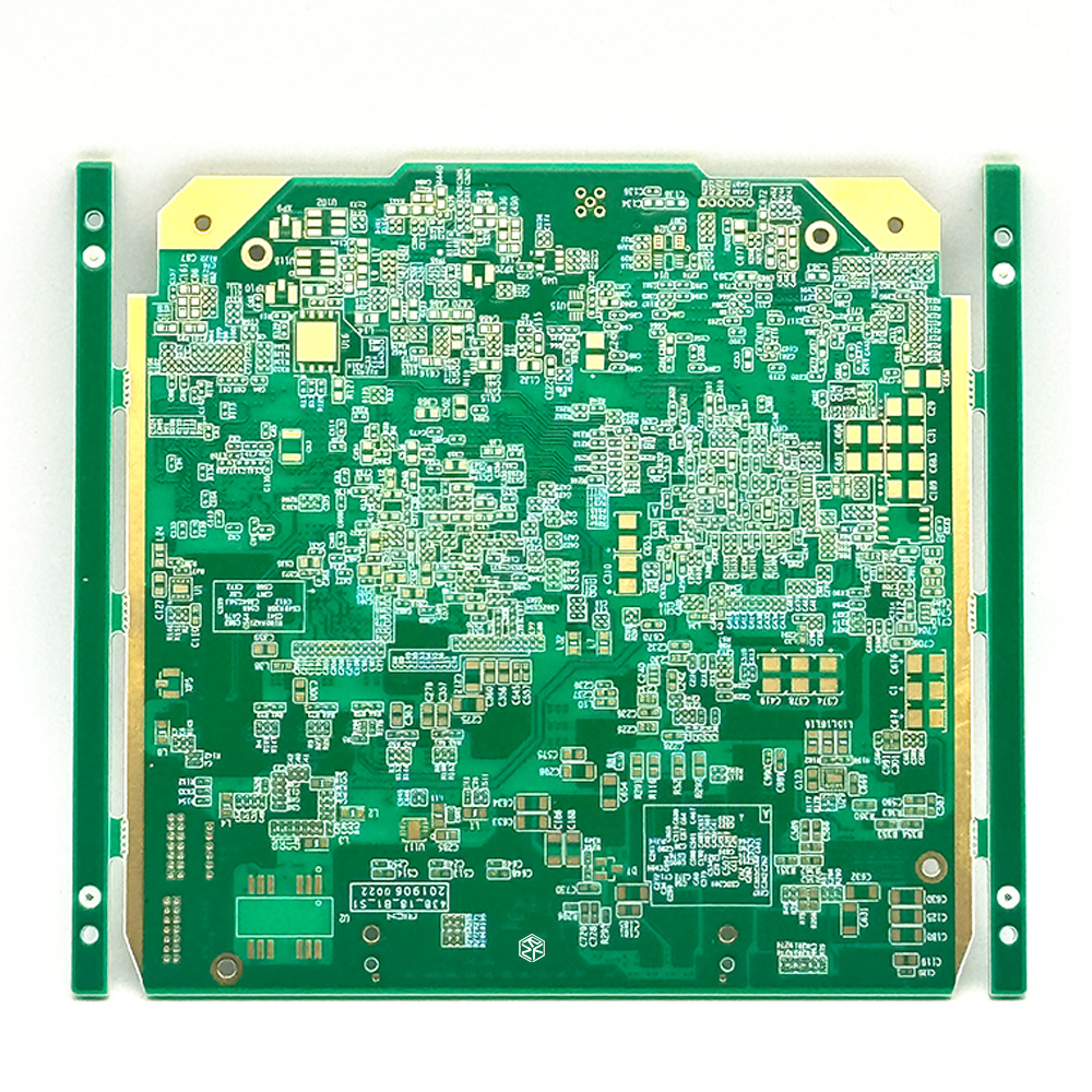
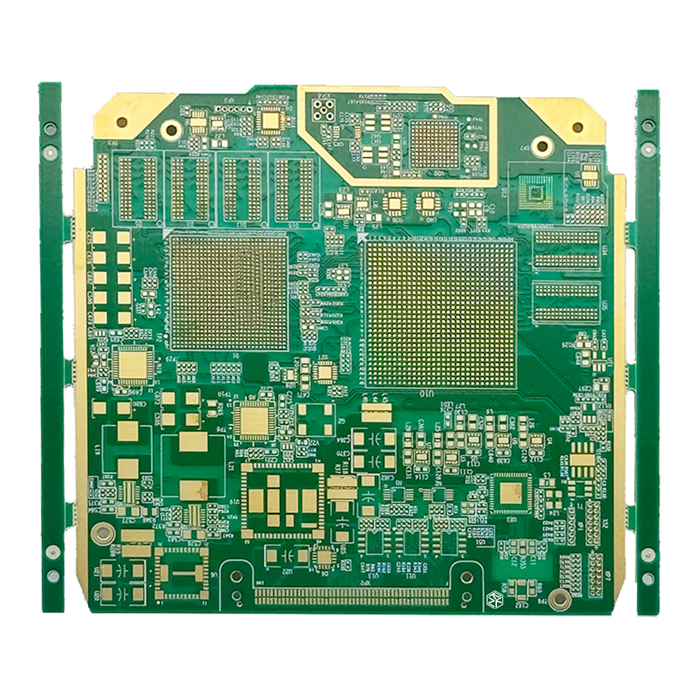
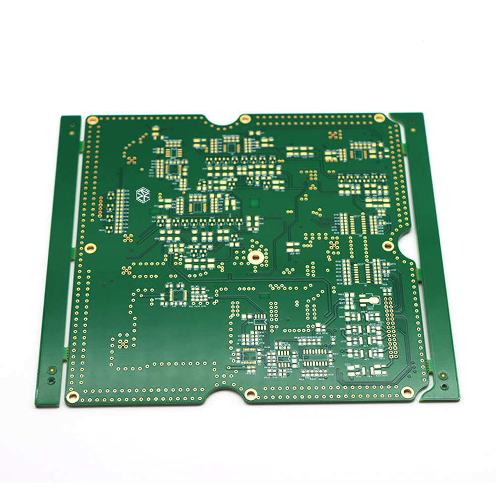
High-frequency Hybrid pressing PCB I 14L impedance


High layer/any layer HDI manufacturer
Quality
Quality Management System:ISO 9001: 2015、 ISO14001:2015、IATF16949: 2016、OHSAS 18001: 2007、QC080000:2012SGS 、RBA、CQC、WCA & ESA、SQ MARK、Canon GA、Sony GP
PCB quality standard:IPC 1 、IPC 2、IPC 3 、GJB 362C-2021,AS9100
PCB major manufacturing process:IL/lmage、PatternPlating、I/L AOI、B/Oxide、Layup、Press、LaserDrilling、Drilling、PTH、PanelPlating、O/Llmage、PanelPlating、SESEtching、O/L AOI、S/Mask、Legend、SurfaceFinshed(ENIGENEPIG、Hard Gold、Soft Gold、HASL、LF-HASL、lmm Tin、lmm Silver、OSP)、Rout 、ET、FV
Inspection equipment test items
oven:thermal energy storage testing
Ion contamination level testing machine:Ionic cleanliness test
salt spray testing machine:Salt spray test
DC high-voltage tester:voltage withstand test
megger:insulation resistance
universal tensile machine:peel strength test
CAF:Ion migration testing, improving PCB substrates, improving PCB processing, etc.
OGP :Using non-contact 3D image measuring instruments, combined with XYZ axis moving platform and automatic zoom mirror, utilizing image analysis principles to process image signals by computer, the measurement of geometric dimensions and positional tolerances can be quickly and accurately detected, and CPK values can be analyzed.
On line resistance control machine:control resistance TCT test Common failure modes, understanding the potential factors that may cause damage to system equipment and components to confirm whether the product is correctly designed or manufactured
cold and thermal shock box:cold and thermal shock test, high and low temperature
constant temperature and humidity chamber:Electrochemical corrosion&surface insulation resistance testing
solder pot:solderability test
RoHS:RoHS test
impedance tester:AC impedance and power loss values
electrical testing equipment:Test the circuit continuity of the product
flying needle machine:High voltage insulation and low resistance conducting test
Fully automatic hole inspection machine:Check for various irregular hole types, including round holes, short slot holes, long slot holes, large irregular holes, porous, few holes, large and small holes, and hole plug inspection functions
AOI:AOI automatically scans PCBA products through high-definition CCD cameras, collects images, compares test points with qualified parameters in the database, and after image processing, checks for small defects that may be overlooked on the target PCB. There is no escape from circuit defects
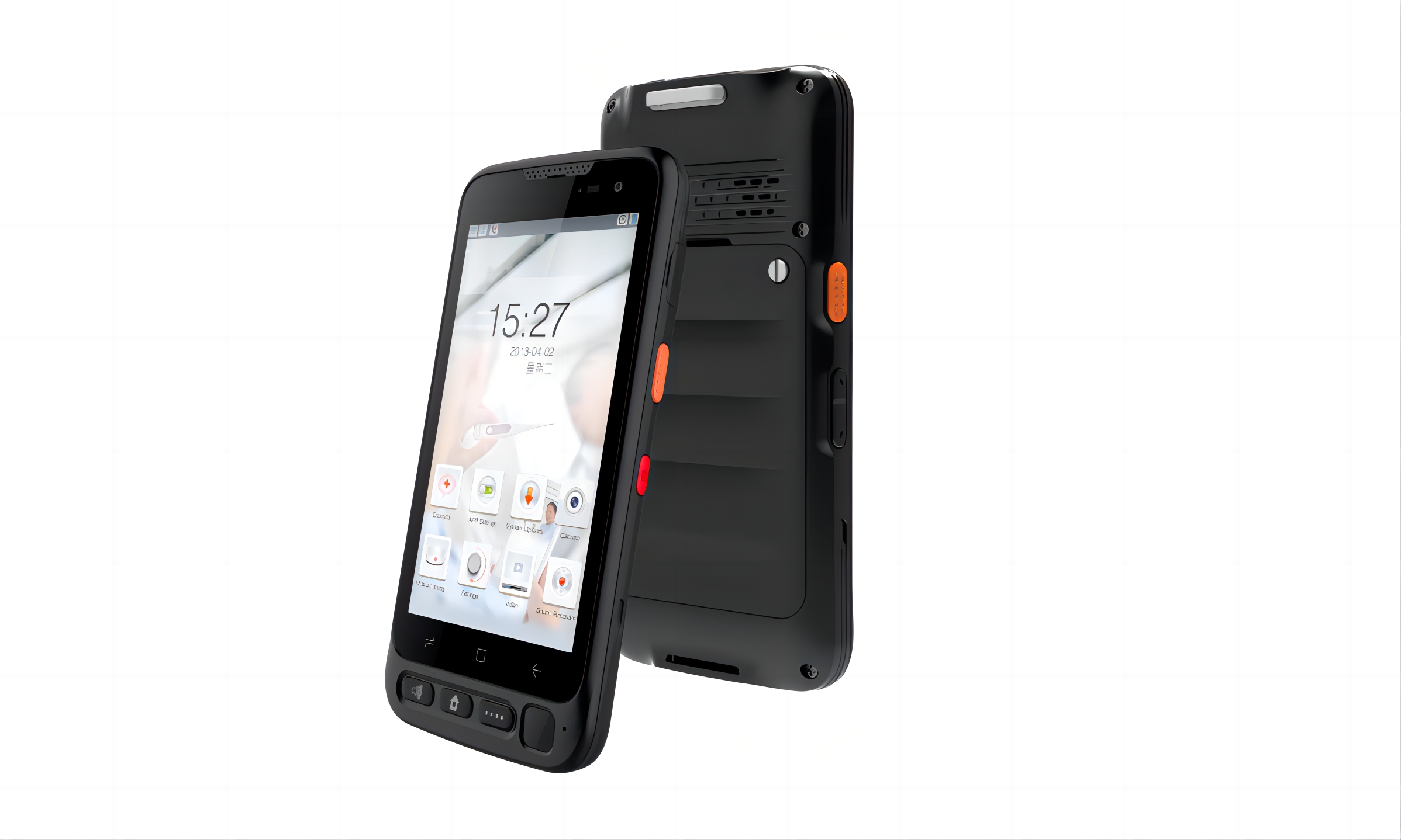
Application (see attached figure for details)
1. 5G Telecommunications
Application: High-frequency hybrid pressing PCBs are critical in 5G base stations, antennas, and RF modules due to their ability to handle high-speed signals and minimize signal loss. The 14-layer impedance control ensures precise signal integrity, while any-layer HDI technology allows for compact, high-density designs.
Key Features: Low dielectric loss, high thermal stability, and excellent impedance matching.
2. Aerospace and Defense
Application: Used in radar systems, satellite communication, and avionics. The multilayer PCB structure supports complex circuitry, and the high-frequency capabilities ensure reliable performance in extreme environments.
Key Features: High reliability, resistance to vibration, and ability to operate in wide temperature ranges.
3. Medical Imaging and Diagnostics
Application: Essential in MRI machines, CT scanners, and ultrasound equipment. The 14-layer impedance control ensures accurate signal transmission, while HDI technology enables miniaturization of complex circuits.
Key Features: High signal integrity, compact design, and compatibility with high-frequency sensors.
4. Automotive Electronics (ADAS and EV Systems)
Application: Used in Advanced Driver Assistance Systems (ADAS), electric vehicle (EV) power management, and infotainment systems. High-frequency PCBs support high-speed data transfer for sensors and cameras.
Key Features: High thermal conductivity, durability, and ability to handle high-power applications.
5. IoT and Smart Devices
Application: Found in smart home devices, wearables, and industrial IoT sensors. Any-layer HDI PCBs enable compact, lightweight designs, while high-frequency capabilities ensure fast data transmission.
Key Features: Miniaturization, low power consumption, and high-speed connectivity.
6. Data Centers and Cloud Computing
Application: Used in servers, switches, and high-speed networking equipment. The 14-layer impedance control ensures minimal signal loss, and hybrid pressing technology supports high-speed data transfer.
Key Features: High bandwidth, thermal management, and reliability for 24/7 operation.
7. Consumer Electronics
Application: Found in smartphones, tablets, and gaming consoles. Any-layer HDI PCBs allow for thinner and lighter devices, while high-frequency capabilities support 5G and Wi-Fi 6/6E connectivity.
Key Features: High-density interconnects, excellent signal integrity, and compact form factor.
8. Industrial Automation and Robotics
Application: Used in PLCs (Programmable Logic Controllers), motor drives, and robotic control systems. High-frequency PCBs ensure precise control signals, and multilayer designs support complex circuitry.
Key Features: High durability, resistance to EMI, and ability to handle high-power loads.
9. Military Communication Systems
Application: Critical in secure communication devices, encrypted data links, and battlefield management systems. The 14-layer impedance control ensures reliable signal transmission in harsh environments.
Key Features: High reliability, resistance to interference, and ability to operate in extreme conditions.
10. High-Performance Computing (HPC)
Application: Used in supercomputers, AI accelerators, and GPU boards. High-frequency hybrid pressing PCBs support ultra-fast data processing, and any-layer HDI technology enables high-density interconnects.
Key Features: High-speed signal transmission, thermal management, and scalability for complex designs.
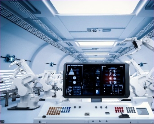
Application
HDI PCBs are used in a wide range of fields such as mobile phones, digital cameras, AI, IC carriers, medical equipment, industrial control, laptops, automotive electronics, robots, drones, etc.