Leave Your Message
-
E-mail
-
Whatsapp
-
Message
Precision-engineered PCBs purpose-built for EV charging infrastructure — from onboard chargers to DC fast-charge stations

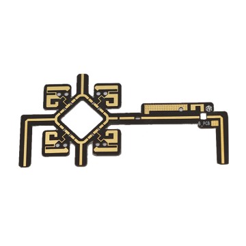
As the global automotive industry undergoes an unprecedented electrification revolution, the demand for robust, high-performance automotive circuits for charging infrastructure has surged to the forefront of electronics engineering. These circuits form the electronic backbone of every EV charging solution — from compact Level 1 home chargers to ultra-fast 350 kW DC public stations — managing power conversion, signal integrity, thermal control, communication protocols, and safety monitoring in real time.
Unlike conventional automotive electronics, charging infrastructure circuits must simultaneously handle high-voltage DC bus management (up to 1,000V), bidirectional power flow for V2G (Vehicle-to-Grid) applications, galvanic isolation, EMI suppression across wide frequency bands, and compliance with standards such as IEC 61851, SAE J1772, CHAdeMO, CCS, and GB/T. This demands a new generation of high-frequency hybrid PCBs, impedance-controlled multilayer boards, and flexible printed circuits engineered to the most exacting tolerances.
⚡ Key Insight: The global EV charging infrastructure market is projected to exceed USD 140 billion by 2030, driving exponential growth in demand for advanced automotive-grade circuit boards capable of managing high-voltage, high-frequency, and thermally demanding environments.
Today's charging infrastructure ecosystem spans multiple commercial and industrial segments, each placing distinct demands on circuit design and manufacturing:
Operators such as Tesla Supercharger, Ionity, ChargePoint, and EVgo deploy thousands of 150–350 kW DC fast chargers globally. The power electronics inside these units — including LLC resonant converters, active PFC stages, and bidirectional DC-DC converters — rely on multilayer high-frequency PCBs with controlled impedance, low-loss dielectrics (Rogers RO4350B, Shengyi S1000-2M), and precision copper pour for thermal management. Signal integrity at switching frequencies above 100 kHz demands hybrid laminate constructions that minimize dielectric loss tangent.
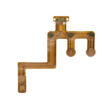
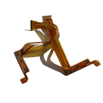
Every battery electric vehicle contains an OBC that converts AC grid power to DC for battery charging. Modern OBCs operate at 6.6 kW to 22 kW, with next-generation units pushing 11–22 kW at 800V architecture. The PCB inside an OBC must survive automotive temperature cycling (−40°C to +125°C), vibration, and humidity while maintaining tight impedance control for GaN/SiC gate-driver circuits switching at 500 kHz–1 MHz. Flexible PCBs and rigid-flex designs are increasingly used to reduce connector count and improve mechanical reliability.
Wireless EV charging (SAE J2954 standard) at 3.7–22 kW uses resonant coil systems operating at 85 kHz. The ground-assembly and vehicle-assembly electronics require RF-grade PCBs with stable dielectric constant (εr) across temperature ranges to maintain coupling efficiency. Millimeter-wave sensing circuits are also integrated for foreign object detection and vehicle alignment.
Bidirectional chargers enabling Vehicle-to-Grid (V2G) and Vehicle-to-Home (V2H) functionality require power-line communication (PLC) circuits, millimeter-wave modules, and secure communication chipsets on the same board. Millimeter-wave power-line communication PCBs, such as those developed by Rich Full Joy Electronics, play a pivotal role in enabling high-speed data exchange across the grid while simultaneously managing power flow.
Six key technological trajectories reshaping automotive circuit design for next-generation charging infrastructure
Gallium Nitride and Silicon Carbide devices switch at higher voltages and frequencies with lower losses, demanding PCBs with ultra-low parasitic inductance, tight impedance control, and thermally conductive substrates — precisely where hybrid high-frequency laminates excel.
Next-generation EVs (Porsche Taycan, Hyundai Ioniq 6, Kia EV6) use 800V battery systems enabling 350 kW charging. This requires PCB insulation systems rated for higher creepage/clearance distances and dielectric materials with superior partial-discharge resistance.
As grids demand flexibility, V2G-capable chargers require bidirectional power electronics with advanced communication interfaces (ISO 15118, OCPP 2.0.1). PCB designs must integrate both high-power and high-frequency communication circuits in a single robust assembly.
Dynamic wireless charging for EVs on highways and static pads in parking lots require millimeter-wave sensing PCBs for precise alignment and safety. Rogers-based RF laminates with stable εr at 77–79 GHz are essential for foreign object detection circuits.
Charging stations are embedding edge-AI processors for real-time fault prediction, thermal monitoring, and dynamic load balancing. This drives demand for high-density multilayer PCBs combining RF, digital, and power domains on a single board with stringent EMI shielding.
Modern charging stations use hot-swappable power modules (10–30 kW each) for scalability and redundancy. Each module's PCB must meet automotive-grade reliability (IATF 16949), vibration resistance, and conformal coating requirements for outdoor deployment.
How advanced automotive circuit boards enable each layer of the charging infrastructure ecosystem
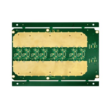
The OBC is the most thermally and electrically demanding board in an EV. Multilayer hybrid PCBs with Rogers RO4350B cores provide low-loss signal routing for GaN gate drivers while FR4 or S1000-2M layers handle structural rigidity and thermal vias. Impedance-controlled traces ensure clean PWM signal integrity at 500 kHz+, preventing shoot-through in half-bridge topologies.
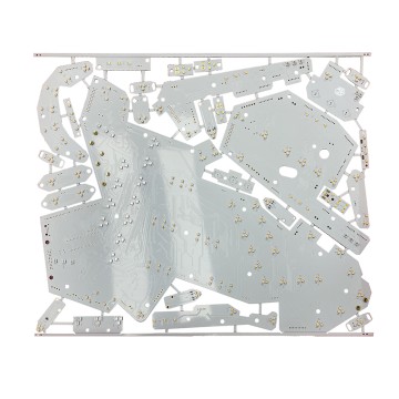
DC fast chargers use multi-phase interleaved PFC and LLC resonant converters. The PCB must route high-current copper (3–6 oz) for power paths while maintaining signal-layer integrity for control loops. 6-layer and 8-layer hybrid PCBs with embedded copper planes for thermal spreading are the industry standard for 150–350 kW units.
Every smart charger contains a communication board managing OCPP, ISO 15118 (Plug & Charge), Modbus, CAN bus, and cellular/Wi-Fi connectivity. These boards require RF-grade sections for antenna feeds, high-speed differential pairs for Ethernet, and robust ESD protection — all achievable with flexible PCBs or rigid-flex assemblies.
The BMS communicates cell voltage, temperature, and state-of-charge data to the charger via isolated CAN or LIN interfaces. Precision analog front-end circuits on the PCB require tight impedance matching and low-noise power planes. FPC double-sided boards are widely used for space-constrained BMS modules in battery packs.
Millimeter-wave power-line communication (PLC) boards enable real-time energy management across charging networks. These boards integrate high-frequency RF circuits operating at GHz frequencies with power-domain isolation, demanding the most advanced hybrid laminate constructions and via-in-pad technology for dense component placement.
Autonomous drones equipped with thermal cameras and RF sensors are increasingly deployed for charging station inspection and maintenance. Drone circuit boards require ultra-lightweight multilayer PCBs with high-density interconnects, combining flight-control MCUs, motor-driver ICs, and RF communication modules on a single rigid-flex assembly.

Based in China and looking at the global market, Shenzhen Rich Full Joy Electronics Co., Ltd. has been committed to industry development for 20 years. The company is a national high-tech innovative enterprise that combines focus and expertise. It's also an important enterprise incubation base in China. We specialize in providing customers with one-stop intelligent electronic manufacturing services, including scientific research, PCB design, PCB manufacturing, PCB assembly (including SMT, DIP, Programming and testing) and component selection.
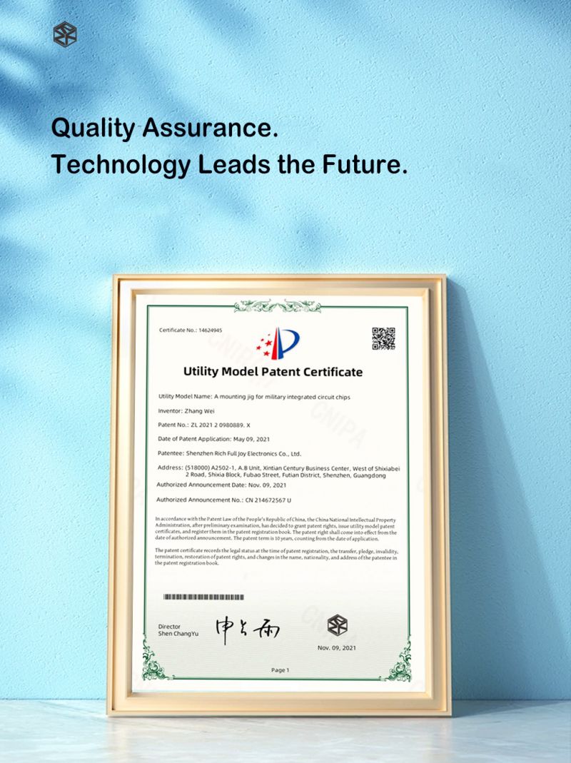
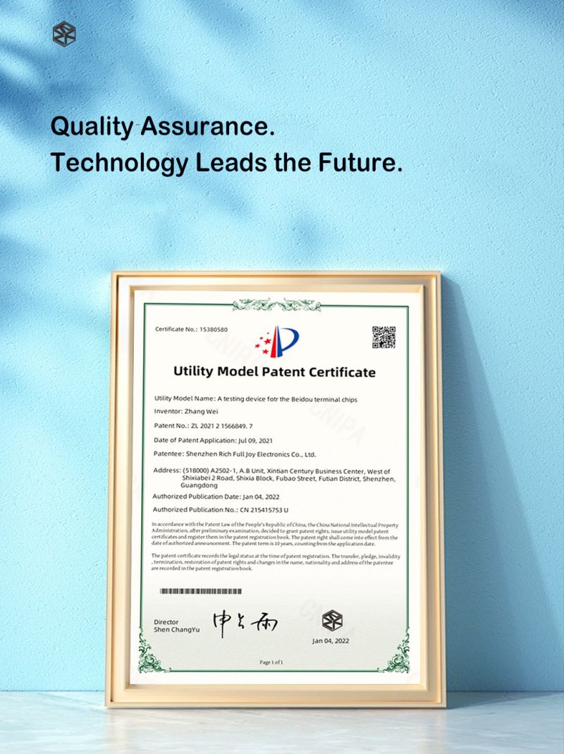
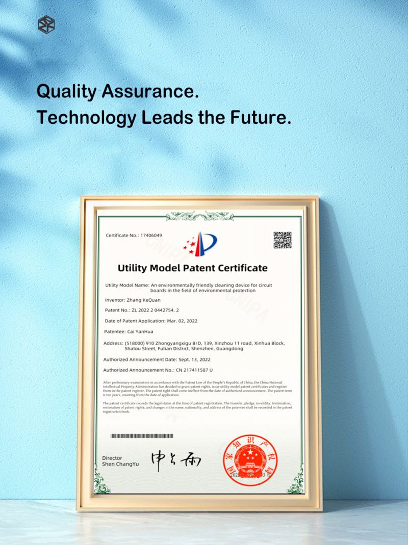
Technological innovation is the core competitiveness of enterprises. We've obtained multiple invention and utility model patents, and has passed various international standard certifications such as ISO9001, IATF16949, ISO14001, UL, CQC, REACH, RoHS, COC, as well as the GJB9001C-2017 standard certification for weapon and equipment quality management system. We've provided high-quality and reliable products to multiple research institutions, universities, and assisted customers in identifying design issues and providing reasonable suggestions and processing parameters.
We not only publish technical papers, but also actively participate in domestic and overseas technology exchange conferences to spread academic value and cutting-edge technological innovation. We regularly communicate with customers and strive to provide them with the best solutions.
Full automotive quality management system certification ensures every PCB for charging infrastructure meets the highest standards for process control, traceability, and reliability over the product lifecycle.
Specialized capability in Rogers RO4350B, Shengyi S1000-2M, and hybrid pressing — essential for GaN/SiC gate-driver circuits and RF communication boards in modern EV chargers.
From PCB design review and DFM analysis through multilayer fabrication, SMT assembly, functional testing, and conformal coating — a complete manufacturing solution under one roof for faster time-to-market.
Our intellectual property portfolio reflects decades of R&D investment in high-frequency, RF, and automotive-grade circuit technologies



















Explore our full portfolio of high-frequency, RF, and flexible PCB solutions engineered for EV charging and smart energy applications