Leave Your Message
-
E-mail
-
Whatsapp
-
Message
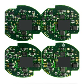
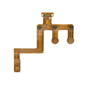
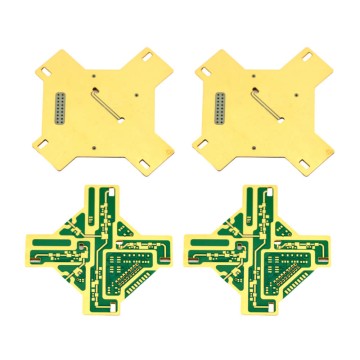
Explore our precision-engineered PCB products designed for high-performance ADAS charging station environments.
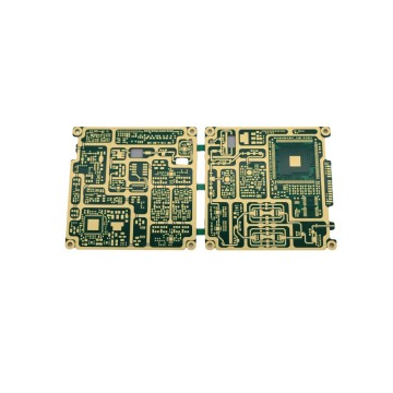
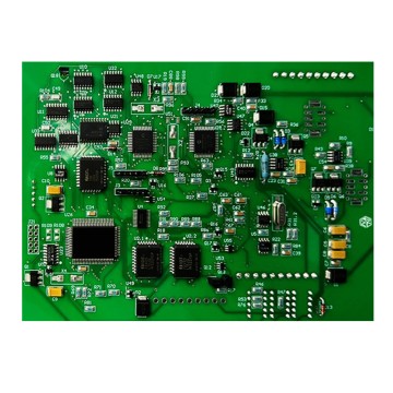
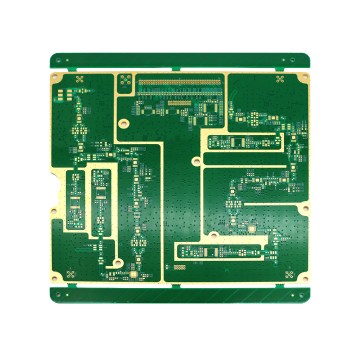

Understanding the critical role of advanced PCB design in modern ADAS-integrated EV charging infrastructure.
As the automotive industry accelerates toward full electrification and autonomous operation, the demand for highly reliable, thermally stable, and electromagnetically compliant Charging Station PCBs for ADAS Systems has never been greater. These specialized printed circuit boards serve as the neural backbone of EV charging infrastructure, enabling seamless communication between charging hardware and the vehicle's Advanced Driver Assistance Systems.
Unlike conventional charging PCBs, ADAS-integrated designs must handle simultaneous high-voltage power delivery, real-time sensor data processing, V2X (vehicle-to-everything) communication, and safety-critical failsafe logic — all within a compact, ruggedized form factor. This demands multi-layer board architectures, hybrid dielectric materials, and ultra-fine trace routing that can sustain signal integrity at frequencies exceeding 5 GHz.
The global EV charging station market is projected to surpass $140 billion by 2030, with ADAS-compatible smart charging representing the fastest-growing segment. Manufacturers and system integrators are now prioritizing PCB suppliers capable of delivering boards that meet ISO 26262 functional safety standards, AEC-Q100 automotive qualification, and IPC Class 3 workmanship — simultaneously.
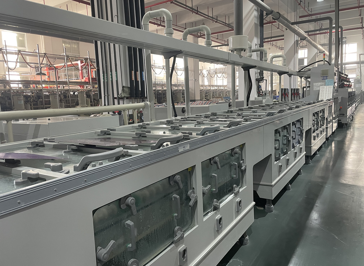
Our engineering team delivers cutting-edge PCB solutions that meet the most demanding ADAS charging station requirements.
Engineered for DC fast charging up to 350kW, our PCBs integrate robust power planes, controlled impedance traces, and advanced thermal vias to manage extreme current loads safely and efficiently across all ADAS charging modes.
Incorporating Rogers RO4350B hybrid substrates, our boards support DSRC, C-V2X, and 5G NR communication protocols essential for ADAS-to-charger handshaking, remote diagnostics, and over-the-air update delivery.
Every ADAS charging station PCB is designed with ASIL-B to ASIL-D compliance in mind, featuring redundant signal paths, fault detection circuits, and EMI shielding layers that ensure fail-safe operation in all environmental conditions.
Using TG170 FR-4 and high-Tg materials, our boards maintain dimensional stability and electrical performance from -40°C to +125°C, critical for outdoor charging stations exposed to extreme climatic variations.
Supporting line/space down to 2mil and via-in-pad technology, our HDI PCBs enable the dense component integration required by ADAS sensor fusion modules, LiDAR interface boards, and radar signal processors.
All charging station PCBs undergo 100% AOI, X-ray inspection, ICT, and flying probe testing. Full traceability documentation, PPAP packages, and IATF 16949 quality management ensure automotive-grade reliability from prototype to mass production.
Key developments shaping the commercial and industrial landscape of intelligent EV charging PCB technology.
Level 3–5 autonomous vehicles require charging stations equipped with ADAS-aware PCBs that can communicate vehicle position, battery state, and docking alignment data in real time. Inductive and robotic charging systems are driving demand for ultra-low-latency PCB designs with sub-microsecond response times.
Municipal EV fleets and ride-sharing operators are deploying ADAS-integrated charging hubs that collect telematics data, optimize charging schedules via AI, and interface with city-wide traffic management systems — all enabled by intelligent multi-layer PCBs with IoT connectivity modules.
Vehicle-to-Grid (V2G) systems require charging station PCBs capable of managing bidirectional power flow with millisecond switching precision. This demands advanced power electronics integration, GaN/SiC device compatibility, and signal isolation layers that prevent grid noise from corrupting ADAS sensor data.
Embedded AI processors on charging station PCBs now monitor component health, predict failure modes, and trigger preventive maintenance alerts. These edge-AI boards integrate NPU accelerators, high-speed memory interfaces, and secure communication channels for cloud-connected diagnostics.
The rollout of 5G infrastructure is enabling ultra-reliable low-latency communication (URLLC) between ADAS vehicles and charging stations. PCBs must now incorporate 5G mmWave antenna arrays, beamforming circuits, and advanced RF shielding to support this next-generation connectivity standard.
Logistics warehouses, airports, and port facilities are deploying high-density ADAS-compatible charging arrays for autonomous guided vehicles (AGVs) and electric ground support equipment. These industrial applications demand PCBs with enhanced vibration resistance, conformal coating, and IP67-rated assembly processes.
How charging station PCBs power the most advanced ADAS use cases across industries.
Companies like Waymo, Cruise, and Baidu Apollo operate large robotaxi fleets that require 24/7 autonomous charging without human intervention. Charging station PCBs in this scenario must handle encrypted vehicle authentication protocols (ISO 15118), automated plug engagement confirmation, and real-time ADAS system health reporting — all within a single integrated board design.
The PCB must interface with ultrasonic proximity sensors, optical alignment cameras, and robotic arm controllers simultaneously, requiring a minimum of 12 signal layers with controlled differential impedance and shielded power planes to prevent cross-domain interference.


The Megawatt Charging System (MCS) standard for electric semi-trucks delivers up to 3.75MW of power, placing extraordinary demands on charging station PCBs. These boards must manage multi-phase power conversion, liquid-cooled busbar interfaces, and ADAS-level safety interlocks that prevent charging under unsafe vehicle conditions detected by onboard sensor arrays.
Our engineering team has developed specialized PCB stackups using hybrid Rogers/FR-4 constructions with embedded copper coin technology for superior thermal dissipation — enabling reliable operation at ambient temperatures up to 85°C in direct sunlight exposure scenarios common at highway charging depots.
Partner with a PCB manufacturer that understands the full complexity of ADAS-integrated charging station design. From single prototype to high-volume production, our team of 800+ engineers delivers ISO 26262-compliant, AEC-Q100-qualified PCBs that meet every technical and regulatory requirement of your next-generation charging infrastructure project.
Explore Our ADAS PCB Solutions →
Over 20 years of PCB R&D, design and production. With a team of over 800 design engineers, striving for excellence, our service network has spread all over the world.
As a company involved in the development and design of multiple scientific research products, our products are widely applied in various fields such as aviation, aerospace, automotive electronics, medical devices, industrial control, mobile terminal devices, servers, smart homes, AI applications, new energy, mini LED and testing instruments, etc.
We have a high-quality and highly capable technology R&D team, adhering to the development concept of high-end brands and products, and serving global customers. Our products are exported to various regions of the world.
We continue to lead in the production of small batches, multiple varieties, high difficulty and high-precision products in differentiated market competition. We have complete sets of advanced automatic production and testing equipment, strictly control every process, and are committed to the meticulous and perfect quality of products. All products strictly adopt international IPC standards for production and inspection, with 24-hour high quality one-on-one service.
We uphold the spirit of craftsmanship to build intelligent manufacturing, leading the industry with technology and driven by technological innovation. We'll strive for excellence and become a leader in the industry, continuously strengthening our core competitiveness and establishing a leading position in various fields.
Our commitment to ADAS charging station PCB excellence is reflected in every board we manufacture — from the careful selection of substrate materials to the final electrical validation testing that ensures your charging infrastructure performs flawlessly in the most demanding real-world conditions.
The values that drive our commitment to ADAS charging PCB excellence.
Every charging station PCB we produce is backed by transparent processes, honest engineering assessments, and uncompromising quality standards that our ADAS system customers can trust completely.
From embedded AI diagnostics to GaN-compatible power layers, we continuously invest in R&D to ensure our ADAS charging PCB solutions stay ahead of industry evolution and regulatory requirements.
Superior quality and excellent service meet clients' needs and ideas, help them win the market to achieve success. Our global service network ensures responsive support for ADAS charging projects in every major automotive market worldwide.
Browse our complete range of advanced PCB solutions engineered for ADAS charging and intelligent automotive applications.