


01


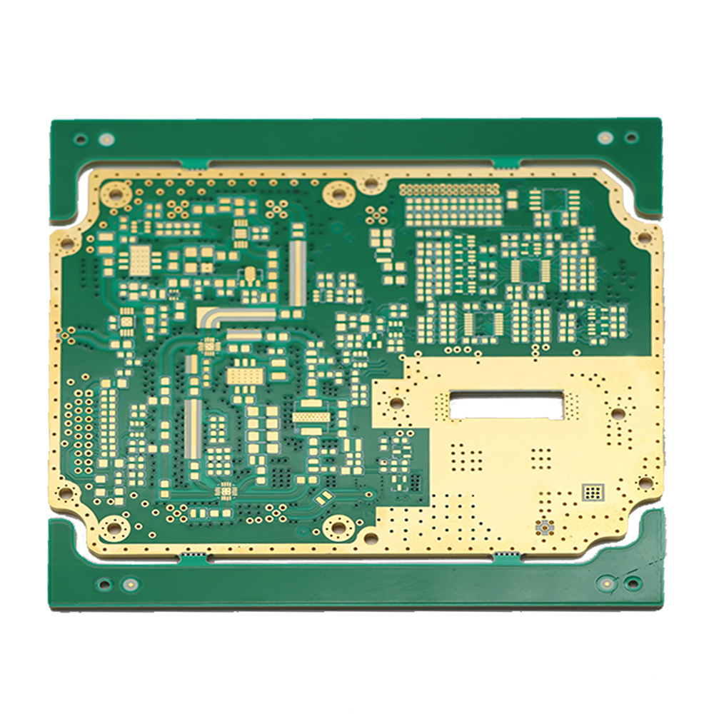
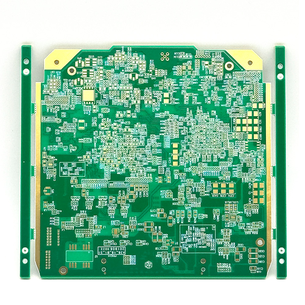
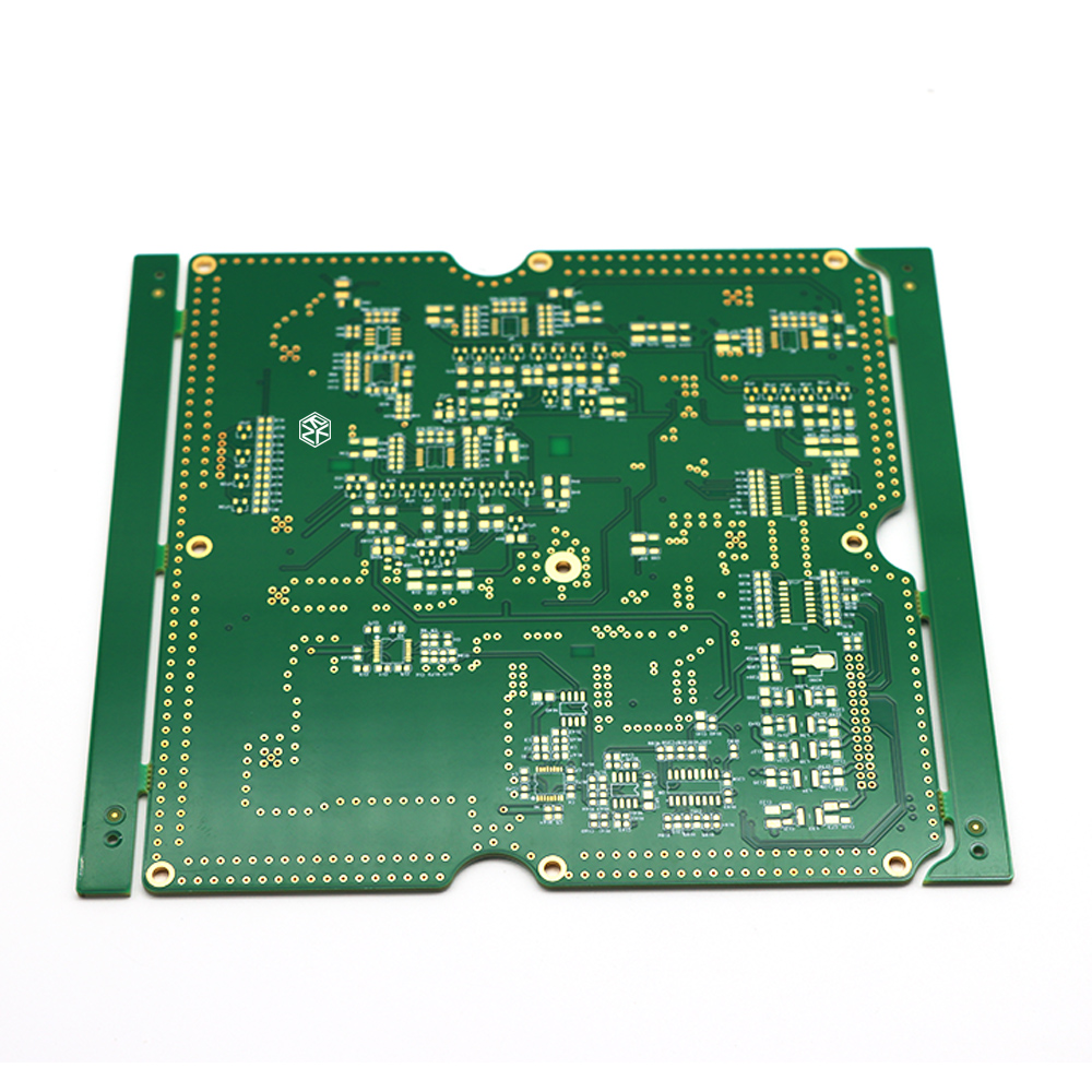
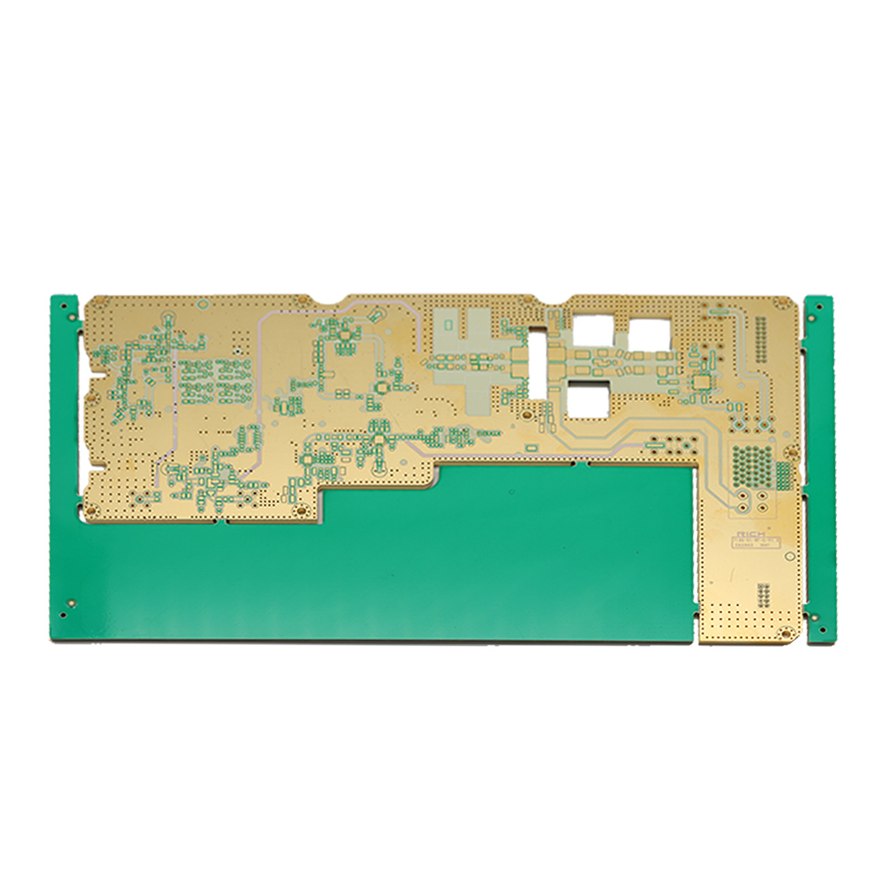
Half-Hole PCB,5G Module PCB


Applications of 5G Modules

5G modules are crucial components in the advancement of wireless communication technology. They are widely used in various applications, including:
Smartphones and Tablets: Integrating 5G modules enhances internet speed and connectivity, offering users a superior mobile experience.
IoT Devices: 5G modules enable seamless connectivity for Internet of Things (IoT) devices, facilitating smart homes, smart cities, and industrial automation.
Automotive Systems: These modules support connected car technologies, including real-time navigation, vehicle-to-everything (V2X) communication, and autonomous driving features.
Healthcare Devices: 5G modules improve telemedicine and remote patient monitoring, allowing for faster data transmission and real-time diagnostics.
Industrial Automation: 5G modules enhance automation processes in factories, providing reliable and fast data transfer for smart manufacturing.
Augmented and Virtual Reality: They enable high-speed data transfer necessary for immersive AR and VR experiences.
Incorporating 5G modules in these applications ensures high-speed connectivity, low latency, and improved overall performance.
Challenges in Manufacturing 5G Module, Half-Hole PCB
High-Frequency Signal Integrity:
Issue: Ensuring signal integrity for high-frequency 5G signals is challenging due to potential interference and signal loss.
Solution: Use high-frequency materials and precise design techniques to minimize signal degradation.
Half-Hole Accuracy:
Issue: Achieving precise drilling and plating of half-holes can be difficult, impacting connectivity and reliability.
Solution: Implement advanced drilling and plating technology, and maintain strict quality control.

Thermal Management:
Issue: 5G modules generate significant heat, which can affect PCB performance and longevity.
Solution: Incorporate effective thermal management solutions, such as heat sinks and thermal vias.
Component Placement and Alignment:
Issue: Accurate placement and alignment of the 5G module on the PCB are critical to avoid performance issues.
Solution: Utilize automated pick-and-place machines and ensure precise alignment during assembly.
Material Compatibility:
Issue: Compatibility between the PCB substrate, copper layers, and the 5G module can be challenging.
Solution: Select appropriate materials and ensure compatibility through rigorous testing.
Manufacturing Tolerances:
Issue: Maintaining tight tolerances for PCB dimensions and hole sizes is crucial for proper module integration.
Solution: Use high-precision manufacturing equipment and implement thorough inspection processes.
Cost Management:
Issue: The advanced technology required for 5G PCBs can lead to higher production costs.
Solution: Optimize the production process and materials to balance performance and cost.
What is a Half-Hole PCB?

A half-hole PCB (Printed Circuit Board) refers to a type of PCB that incorporates vias with only partial plating or coverage. These half-holes are typically used to connect different layers of the PCB without fully plating the hole, often to save costs or reduce manufacturing complexity.
Characteristics of Half-Hole PCBs:
Design Flexibility: Half-holes can help manage space and routing on a PCB, allowing for more efficient design.
Cost Efficiency: They can reduce manufacturing costs by minimizing the amount of plating required.
Manufacturing Simplicity: They simplify the drilling and plating process compared to fully plated vias.
Common Uses:
Signal Routing: To connect different layers in a multi-layer PCB.
Cost-Effective Solutions: In designs where full plating is not necessary for performance or reliability.
Manufacturing Method for 5G Module, Half-Hole PCB
CDesign and Prototyping:
Schematic Design: Create a detailed schematic of the PCB, incorporating the 5G module and half-hole design requirements.
PCB Layout: Develop the PCB layout, ensuring accurate placement of the 5G module and half-hole through-holes.
Material Selection:
PCB Substrate: Choose a suitable substrate material such as FR4 or high-frequency materials like Rogers for 5G applications.
Copper Thickness: Select appropriate copper thickness for signal integrity and power requirements.

PCB Fabrication:
Photographic Process: Apply a photosensitive film to the PCB substrate and expose it to UV light through a photomask to create the circuit pattern.
Etching: Remove unwanted copper using an etching solution to reveal the PCB traces and half-holes.
Drilling: Drill the half-holes (vias) with precision to ensure accurate alignment and connectivity.
Assembly:
Component Placement: Place the 5G module and other components on the PCB using automated pick-and-place machines.
Soldering: Use reflow soldering or wave soldering techniques to secure the components, including the 5G module, onto the PCB.
Testing and Quality Control:
Electrical Testing: Perform electrical tests to verify connectivity and signal integrity, ensuring that the half-holes and 5G module function correctly.
Inspection: Conduct visual inspections and use X-ray machines to check for defects or soldering issues.
Final Assembly:
Enclosure: Mount the PCB with the 5G module into its final enclosure or housing, ensuring proper thermal management and protection.