


01


Half-Hole PCB Sensor Half-Hole PCB


Plated Half-Hole

A plated half-hole, also known as a castellated hole, is a structure designed along the edges of a PCB resembling serrated edges. It is created by first fabricating standard plated vias and then using a sharp milling tool to cut away part of the hole, leaving half of it intact.
This design is an efficient and convenient method for lateral connectivity, often used in signal circuits and extensively for board-to-board connections. Plated half-holes can be directly soldered to the edges of the main board, saving on connectors and space. For instance, Bluetooth or Wi-Fi modules with plated half-holes can be easily soldered onto a main board as single components, meeting specific requirements without the need for additional wiring, resulting in a clean and straightforward assembly.
While plated half-holes facilitate board-to-board soldering, they are considered a specialized technology in the PCB industry and come with a higher cost. Additionally, the production cycle for these PCBs is relatively longer.
Features of Sensor Half-Hole PCBs
1. Compact Design:
Half-hole PCBs for sensors are designed to be compact, allowing for efficient use of space in small sensor modules. This compactness is crucial for integrating sensors into tight spaces within devices.
2. Efficient Connectivity:
The half-hole design facilitates reliable board-to-board connections, which is essential for sensors that need to interface with other electronic components or boards. This design reduces the need for additional connectors and helps streamline the assembly process.
3. Enhanced Signal Integrity:
Half-holes help maintain signal integrity by minimizing the distance between signal paths and reducing interference. This is particularly important for sensors that rely on accurate data transmission for performance.

4. Cost-Effective Manufacturing:
By utilizing half-holes, manufacturers can often reduce costs associated with connectors and assembly. This is due to the direct soldering capability of half-holes, which simplifies the manufacturing process.
5. Space Optimization:
The use of half-holes allows for better space management on the PCB. This is beneficial in sensor applications where space is limited and efficient layout is critical for functionality and performance.
6. Versatile Applications:
Sensor half-hole PCBs are versatile and can be used in various types of sensors, including environmental sensors, motion sensors, and imaging sensors. Their design accommodates different sensor sizes and mounting requirements.
7. Improved Reliability:
Half-hole PCBs enhance the reliability of sensors by providing a robust connection method. This reduces the risk of mechanical failures and improves the durability of the sensor assemblies.
Manufacturability Design of Half-Hole PCBs
Minimum Half-Hole Size
The minimum manufacturable size for half-holes is 0.5mm, provided that the hole is centered along the edge of the PCB. This means that there must be a 0.25mm area of copper within the PCB to ensure the integrity of the hole. Without this central copper area, the copper on the hole walls may detach during the production process, leading to unplated holes and rendering the final product unusable.
Half-Hole Spacing
For half-hole PCBs, the minimum finished hole diameter is 0.5mm. During the manufacturing process, the hole diameter needs to be compensated. After compensation, the spacing between half-holes must be at least 0.35mm. Therefore, the designed spacing between half-holes should be ≥0.45mm. The corresponding solder pads for the half-holes must be compensated to ensure they are ≥0.25mm. Additionally, there must be a solder mask bridge between the solder mask openings and the solder pads for the half-holes.
Half-Hole Panelization
When panelizing half-hole PCBs, it is essential to leave spacing around the half-holes to facilitate the routing and milling process. This detail is often overlooked during the design phase because few layout engineers have visited PCB factories to understand how half-holes are manufactured. As a result, half-hole products are sometimes panelized without proper spacing, using standard V-CUT methods. This can lead to the copper on the half-holes being pulled off by the V-CUT blade, resulting in unplated holes and rendering the product unusable.
Half-Hole PCB Design Specifications
A. Distance from Half-Hole Pad Edge to Board Edge: ≥1mm
B. Half-Hole Diameter: ≥0.6mm
C. Spacing Between Half-Holes: ≥0.6mm
D. Single-Side Solder Ring for Half-Hole: ≥0.25mm (minimum 0.18mm)
Half-Hole PCB Panelization Specifications
Individual Board Size: The length and width of the half-hole PCB should be >10mm (this applies to the panelized boards as well). Like standard boards, half-hole PCBs can be panelized using V-CUT and tab routing methods.
Edge Treatment: The edges of the half-hole PCB cannot be shaped using V-CUT, as V-CUT can pull off the copper.
How to Design Half-Hole PCBs
Open PCB Design Software: Launch your PCB design software and create a new PCB project.
Select Half-Hole Locations: In the layout editor, choose the locations where you want to add half-holes.
Add Vias: In the layout editor, select the option to “Add Via” or a similar feature.
Set Via Parameters: Configure the via’s diameter and position. Ensure that the via is set to be a half-hole, meaning it has copper coating on only one side.
Adjust Position and Size: Modify the via’s position and size as needed to meet your design requirements.

Products Using Half-Hole PCBs
Bluetooth Modules: Commonly used in various wireless communication devices for connectivity.
Wi-Fi Modules: Found in consumer electronics like laptops and routers to enable wireless internet connections.
Wearable Devices: Such as smartwatches and fitness trackers, where space-saving and efficient board-to-board connections are crucial.
RFID Tags: Utilized in tracking and identification systems, benefiting from compact and efficient PCB designs.
Small IoT Devices: Devices like smart sensors and compact gateways that require miniaturized and effective interconnections.
Camera Modules: Used in mobile phones and other imaging devices, where space constraints and board connectivity are critical.
Automotive Sensors: Compact sensors used in automotive applications for monitoring and control systems.

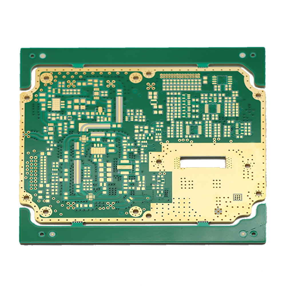
Half-Hole PCB
Half-hole PCBs feature rows of holes drilled along the edge of the PCB. When these holes are copper-plated, the edges are trimmed, resulting in a half-plated appearance along the boundary. This design gives the PCB edge a copper-plated surface look.
In module-type PCBs, half-holes are commonly integrated to facilitate soldering. Due to the small size and diverse functional requirements of modules, half-holes are usually placed along the very edge of the PCB. During the routing process, half of the edge is cut away, leaving only the half-plated holes visible on the PCB.
This design approach enhances the ease of soldering and aligns with the needs of compact, multifunctional modules.
Challenges of Half-Hole PCB Manufacturing
In half-hole processing, if copper burrs remain inside the metallized holes, it can lead to issues such as weak solder joints, cold soldering, and short circuits between pins, especially in rows of half-holes where the spacing is very small and prone to short circuits. During the routing process, problems such as raised copper on the hole walls and residual burrs are common, typically due to insufficient routing tool speed, inadequate bonding between the copper and the hole walls, and excessive copper thickness that leads to incomplete cutting.
Additionally, in the case of metallized half-holes, variations in PCB expansion, drilling precision, and forming accuracy can result in significant size deviations between half-holes on either side of the same unit. This discrepancy poses significant challenges for customers during soldering and assembly.
Reasons for Increased Costs of Half-Hole PCBs
Half-holes involve a specialized manufacturing process. To ensure that there is copper inside the holes, the edges must be routed partway through the process. Additionally, half-hole PCBs are usually very small, which further increases the cost. As a result, non-standard designs come with a non-standard price.