Leave Your Message

Advanced PCB for High-frequency Handheld Devices: The Perfect Integration of Rogers + FR4 TG170, HDI, and Resin Plugging Process

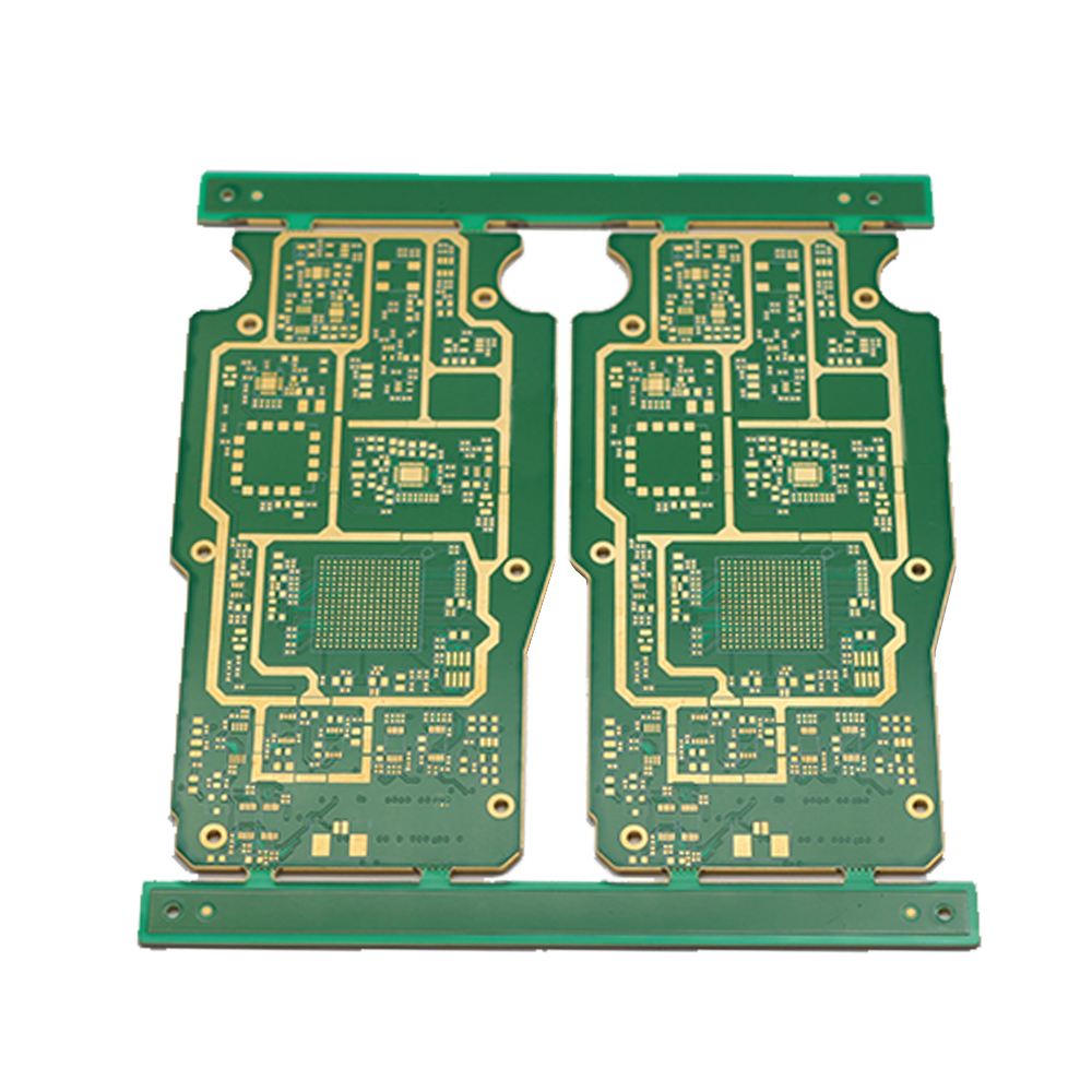
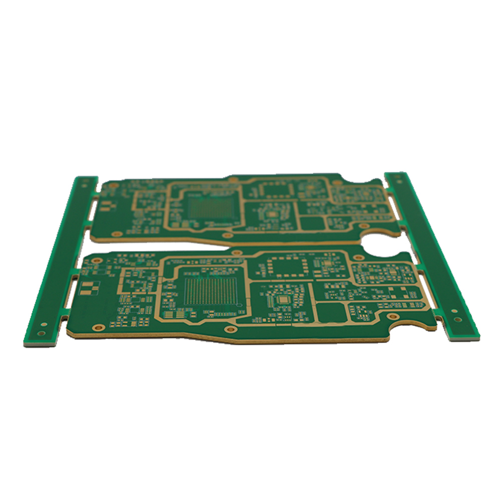
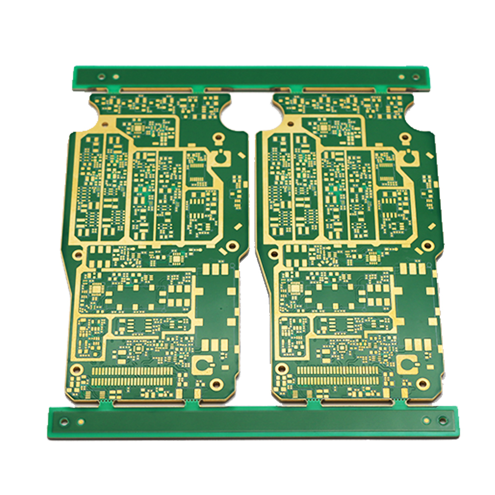
In the field of high-frequency handheld devices, the PCB, as a key component, plays a decisive role in the performance of the equipment. Our PCB for high-frequency handheld devices uses a combination of Rogers + FR4 TG170 materials, combined with HDI (High Density Interconnect) technology and the resin plugging process, which can meet the strict requirements of high-frequency handheld devices for signal transmission, heat dissipation, and space utilization. Rogers materials have excellent high-frequency performance and low-loss characteristics, while FR4 TG170 provides good mechanical strength and electrical insulation. HDI technology enables high-density circuit connections, and the resin plugging process ensures reliable electrical connections and good heat dissipation performance, allowing high-frequency handheld devices to operate stably in complex environments.

    quote now

    What are the Rogers+ FR4 TG170, HDI and resin plugging processes in high-frequency handheld PCBs?
    1

    Our PCB for high-frequency handheld devices adopts unique materials and advanced processes. Rogers materials are renowned for their excellent high-frequency electrical performance. They have a low dielectric constant and low loss tangent value, which can effectively reduce the attenuation and distortion of signals during transmission, making them particularly suitable for processing high-frequency signals. FR4 TG170 is a high-performance glass fiber-reinforced epoxy laminate with a relatively high glass transition temperature (TG170). This enables it to maintain good mechanical properties and electrical insulation even in high-temperature environments, providing stable structural support for the PCB.
    HDI (High Density Interconnect) technology allows for higher-density circuit connections within a limited space. Through the design of fine line pitches and vias, HDI technology can integrate more electronic components, increasing the functional density of the PCB. At the same time, it can also achieve high-speed data transmission to meet the requirements of high-frequency handheld devices for data processing speed.
    The resin plugging process involves filling the vias of the PCB with resin and then curing it. This process not only prevents the oxidation of the copper layer inside the vias, improving the reliability of electrical connections, but also enhances the heat dissipation performance of the PCB. Since the resin has good thermal conductivity, it can effectively transfer heat, ensuring the stability of the PCB during high-frequency operation.

    Excellent High-frequency Performance: The low-loss characteristics of Rogers materials and the high-speed data transmission capability of HDI technology enable high-frequency handheld devices to accurately send and receive signals in complex electromagnetic environments, reducing signal interference and bit error rates, and improving communication quality.
    Reliable Electrical Connections: The resin plugging process ensures the reliability of electrical connections in the vias, preventing signal short circuits and open circuits. At the same time, the fine circuit design of HDI technology also reduces the impedance changes during signal transmission, ensuring the integrity of the signal.
    Good Heat Dissipation Performance: The high glass transition temperature of FR4 TG170 and the heat dissipation advantages of the resin plugging process enable the PCB to effectively dissipate the heat generated during high-frequency operation, avoiding performance degradation and failures caused by overheating, and extending the service life of high-frequency handheld devices.
    Compact Structural Design: The high-density circuit integration capability of HDI technology allows the PCB to achieve more functions within a limited space, meeting the design requirements of high-frequency handheld devices for miniaturization and lightweight, and improving the portability and ease of use of the equipment.
    Quality control is of utmost importance in the manufacturing of PCBs for high-frequency handheld devices. Our PCBs undergo rigorous testing to meet the strict requirements of high-frequency handheld devices. The tests include:
    Electrical Performance Testing: To ensure accurate signal transmission, proper impedance matching, and a stable power supply. This includes testing parameters such as signal integrity, voltage stability, current-carrying capacity, and signal loss at high frequencies.
    Mechanical Performance Testing: To verify the mechanical strength and stability of the PCB, including bending tests, impact tests, and vibration tests, etc., to ensure that the PCB can operate normally under various environmental conditions.
    Thermal Performance Testing: To confirm that the PCB can maintain good performance in high-temperature environments, including thermal cycle tests and thermal resistance tests, etc., to evaluate the heat dissipation capability and high-temperature resistance of the PCB.
    Environmental Stress Testing: To ensure that the PCB can still operate reliably under harsh environmental conditions such as humidity, salt spray, and dust. The protective performance of the PCB is tested by simulating the actual usage environment.
    These tests ensure that our PCBs can operate stably and reliably in applications of high-frequency handheld devices.

    Why choose us for your high frequency handheld station PCB needs?
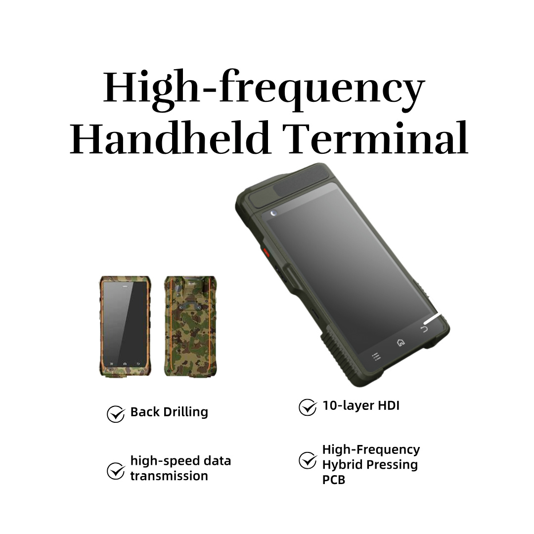
    Profound Expertise in High-frequency PCBs: With years of experience in the design and manufacturing of high-frequency PCBs, we have a deep understanding of the special requirements of high-frequency handheld devices. Our team consists of electronic engineers, circuit designers, and material experts who are proficient in the latest high-frequency technologies and processes, and can provide you with professional solutions.
    Customized Solutions: Each high-frequency handheld device project has unique requirements. According to your specific needs, we provide customized PCB designs, including aspects such as circuit layout, material selection, and process optimization. Our goal is to provide you with the most suitable PCB solution to meet your performance, cost, and time requirements.
    Unparalleled Quality and Reliability: We strictly control every link from raw material procurement to finished product delivery to ensure that every PCB meets the highest quality standards. We adopt advanced manufacturing equipment and processes, such as high-precision laser drilling, automatic surface mounting technology, and X-ray inspection, etc., to ensure the quality and reliability of the PCB.
    Advanced Manufacturing Facilities: We possess advanced manufacturing facilities, including high-precision PCB manufacturing equipment, automated assembly production lines, and comprehensive testing equipment. These facilities enable us to efficiently produce high-quality PCBs and meet your large-scale production needs.
    Timely Delivery and Global Support: We understand the importance of time for your project. We have established an efficient supply chain management system and production planning system to ensure the timely delivery of your PCBs. Our global service team is always ready to provide you with technical support and after-sales service to solve the problems you encounter during the use process.

    2

    Material Selection: We carefully select Rogers and FR4 TG170 materials to ensure that their quality and performance meet our strict standards. At the same time, we also select high-quality copper foils, resins, and other auxiliary materials to ensure the overall performance of the PCB.

    PCB Manufacturing: Our advanced manufacturing process ensures that every PCB can be precisely manufactured. High-precision laser drilling technology is used to create tiny vias, the etching process precisely controls the width and spacing of the circuit lines, and the multi-layer stacking process is strictly aligned to ensure the reliability of electrical connections and the stability of the mechanical structure. Resin Plugging: During the PCB manufacturing process, we adopt an advanced resin plugging process to precisely fill the vias with resin and then cure it. This process requires strict control of the resin filling amount and curing conditions to ensure the electrical performance and heat dissipation performance of the vias. Component Assembly: The component assembly process uses automatic surface mounting technology (SMT) and through-hole technology. We use high-precision chip mounters and soldering equipment to ensure the accurate installation and reliable soldering of electronic components. At the same time, we also conduct in-process quality inspections to promptly detect and solve assembly problems. Testing and Quality Control: Every PCB undergoes comprehensive testing and quality control. In addition to the previously mentioned electrical performance testing, mechanical performance testing, thermal performance testing, and environmental stress testing, we also conduct functional testing and reliability testing to ensure that the PCB can meet the actual usage requirements of high-frequency handheld devices. Final Inspection and Packaging: After the PCB has completed all the tests, we conduct a final inspection to ensure that every PCB meets our quality standards. Then, we use professional packaging materials and methods to package the PCB to prevent damage during transportation.

    Impedance Control: In the PCB design of high-frequency handheld radios, precise impedance control is the key to ensuring signal integrity. We use professional design software and tools to accurately calculate and optimize the impedance of the circuit, ensuring that there is no reflection and distortion of the signal during transmission.
    Signal Routing and Layer Stacking: Since high-frequency handheld radios need to process various signals of different frequencies and types, the design of reasonable signal routing and layer stacking is crucial. We adopt a multi-layer design, route different types of signals separately, and use shielding layers and grounding layers to reduce signal interference. At the same time, we also optimize the signal transmission path to reduce signal transmission delay.
    Thermal Management: High-frequency handheld radios generate a large amount of heat during operation. Effective thermal management is an important factor in ensuring the performance and reliability of the equipment. We have considered the heat dissipation problem in the PCB design and adopted heat dissipation measures such as heat sinks, thermal pads, and thermal vias to effectively dissipate the heat and keep the working temperature of the PCB within a reasonable range.
    Miniaturization and Integration: In order to meet the requirements of miniaturization and lightweight of high-frequency handheld radios, we focus on the integration of components and the optimization of space in the design. By adopting high-density packaging technology and miniaturized electronic components, we can achieve more functions within a limited space while reducing the size and weight of the PCB.
    The PCB of high-frequency handheld radios uses Rogers + FR4 TG170 materials, HDI technology, and resin plugging process, providing a high-performance and reliable solution for high-frequency handheld radios. With our rich experience, professional technology, and strict quality control, we provide you with high-quality PCB products and services to help your high-frequency handheld radio project succeed.
    When you choose us to meet your PCB needs for high-frequency handheld radios, you are choosing a reliable partner. We will wholeheartedly provide you with innovative and reliable solutions.

    Frequently Asked Questions (FAQ)

    3

    Q1: What are the advantages of Rogers materials in the PCB of high-frequency handheld radios?
    Rogers materials have the characteristics of low dielectric constant and low loss tangent value, which enables them to effectively reduce signal attenuation and distortion during high-frequency signal transmission. In high-frequency handheld radios, the accurate transmission of signals is crucial. Rogers materials can ensure the integrity of signals during transmission and improve the communication quality. In addition, Rogers materials also have good thermal stability and chemical stability, which can maintain stable performance under different environmental conditions and extend the service life of the PCB.

    Q2: What is the difference between FR4 TG170 materialand ordinary FR4 material?
    oThe glass transition temperature (TG) of FR4 TG170 material is 170°C, which is higher than that of ordinary FR4 material. This means that FR4 TG170 can maintain better mechanical properties and electrical insulation in a high-temperature environment and is not prone to deformation and damage. In devices such as high-frequency handheld radios that need to work for a long time and may face high-temperature environments, FR4 TG170 material can provide more stable structural support and electrical performance, ensuring the reliability of the PCB.

    Q3: How does HDI technology improve the performance of the PCB of high-frequency handheld radios?
    Through realizing high-density circuit connections, HDI technology can integrate more electronic components within a limited space, increasing the functional density of the PCB. This enables high-frequency handheld radios to have more functions, such as more powerful signal processing capabilities and higher communication rates. At the same time, the fine line pitch and via design of HDI technology can achieve high-speed data transmission, reduce signal transmission delay, and meet the real-time requirements of high-frequency handheld radios. In addition, HDI technology can also reduce interference between signals and improve signal integrity.
    Q4: What help does the resin plugging process provide for the heat dissipation of the PCB of high-frequency handheld radios?
    The resin plugging process fills the vias with resin. Resin has good thermal conductivity and can effectively transfer the heat generated inside the PCB. When the high-frequency handheld radio is working, the electronic components will generate a large amount of heat. Through the resin plugging process, the heat can be quickly conducted to the surface of the PCB through the vias, and then dissipated into the environment through heat sinks or other heat dissipation measures. This helps to reduce the temperature of the PCB, ensure that the electronic components work within a suitable temperature range, and improve the stability and reliability of the equipment.
    Q5: How to ensure the signal integrity of the PCB of high-frequency handheld radios?
    To ensure the signal integrity of the PCB of high-frequency handheld radios, we have taken a variety of measures. First is precise impedance control. By reasonably designing the impedance of the circuit to match the connected components, signal reflection is reduced. Second is reasonable signal routing, routing different types of signals separately to avoid interference between signals. At the same time, we also use shielding layers and grounding layers to further reduce electromagnetic interference. In addition, the selection of high-quality materials and advanced manufacturing processes also has an important impact on signal integrity, such as the low-loss characteristics of Rogers materials and the fine line design of HDI technology. Finally, strict testing and quality control ensure that each PCB meets the requirements of signal integrity.
    Q6: Can the PCB of high-frequency handheld radios be customized?
    Yes, we can customize the PCB of high-frequency handheld radios according to your specific needs. From circuit design, material selection to process optimization, we can carry out personalized customization according to your requirements. Our professional team will communicate with you in depth to understand your project needs and technical requirements, and then provide detailed design plans and technical support to ensure that the customized PCB can meet your performance, cost, and time requirements.

    How to Evaluate the Technical Strength of PCB Suppliers for High-Frequency Handheld Radios?

    Professionalism of the R&D Team: The professional level of the R&D team is an important indicator for measuring the technical strength of PCB suppliers for high-frequency handheld radios. An excellent team should include professional personnel such as electronic engineers, high-frequency circuit experts, and materials engineers. Electronic engineers are responsible for designing circuit schematics to ensure the stable transmission of signals and the realization of functions; high-frequency circuit experts have an in-depth understanding of the characteristics of high-frequency signals and can optimize the circuit layout to reduce signal interference; materials engineers focus on selecting suitable materials, such as Rogers and FR4 TG170, etc., to balance the performance and cost of the materials. Checking the educational background, work experience, and professional qualifications of team members, such as whether they have advanced degrees in related fields, project experience in the field of high-frequency PCBs, and professional certifications, etc., can evaluate the team's ability to solve complex technical problems.
    Technical Achievements and Innovation Ability: The technical achievements of suppliers are an intuitive manifestation of their technical strength. Pay attention to the quantity and quality of patents related to high-frequency PCBs owned by suppliers, especially patents in the application of Rogers materials, improvement of HDI technology, optimization of the resin plugging process, etc. Technical awards are also an important indicator for measuring innovation ability. Suppliers who have won well-known industry awards often have a leading edge in technology. In addition, check the academic papers and technical reports published by suppliers to understand their research depth and breadth in the field of high-frequency PCBs and whether they can promptly apply new technologies to products. The innovation ability is also reflected in the R&D speed of new products. Suppliers who can quickly respond to market demands and launch products with higher performance and competitiveness are more trustworthy.
    Advancement of Production Equipment and Processes: Advanced production equipment is the basis for ensuring the quality and production efficiency of PCBs for high-frequency handheld radios. High-precision laser drilling equipment can create tiny vias, increasing the wiring density of the PCB; fully automatic chip mounters can achieve high-speed and high-precision component mounting, ensuring the quality and consistency of soldering. Understand whether the supplier adopts advanced manufacturing processes, such as multi-layer board lamination processes, surface treatment processes, etc., and whether these processes can meet the special requirements of high-frequency PCBs. For example, in high-frequency PCBs, the surface treatment process has an important impact on signal transmission and corrosion resistance. Adopting advanced surface treatment processes can improve the performance and reliability of the PCB.
    Perfection of the Quality Control System: A complete quality control system is the key to ensuring the quality of PCBs for high-frequency handheld radios. Suppliers should follow international standards and industry norms, such as the ISO 9001 quality management system, IPC-related standards, etc. From the inspection of raw material procurement, on-line detection during the production process to the final testing of the finished product, each link should have clear detection items and standards. For example, conduct strict quality inspections on raw materials such as Rogers and FR4 TG170 to ensure that their performance meets the requirements; during the production process, use advanced means such as X-ray inspection and 3D optical inspection to comprehensively inspect the PCB and promptly detect and eliminate quality problems. Through strict quality control, suppliers can provide high-quality and reliable PCB products.
    Technical Service Ability: High-quality technical service is an important manifestation of the comprehensive strength of suppliers. In the product selection stage, suppliers should be able to provide professional technical advice and solutions according to customers' needs and application scenarios, helping customers choose suitable PCB products. During the product use process, suppliers should have the ability to respond quickly and solve problems, and be able to provide timely technical support and after-sales service. For example, provide 7×24-hour technical consultation services and solve the technical problems encountered by customers through remote diagnosis or on-site services. Good technical service can enhance customers' trust in suppliers and improve customer satisfaction.
    PCB Design of High-Frequency Handheld Walkie-Talkie
    Question: In the PCB design of a certain high-frequency handheld walkie-talkie, how is the impedance control of the radio frequency (RF) signal transmission line carried out?
    Answer: Calculated by the design software, when the thickness of the FR4 medium is 0.8mm, the width of the microstrip line with an impedance of 50Ω is designed to be 3.3mm. At the same time, the stripline structure is adopted to transmit some differential signals, making its characteristic impedance reach 100Ω, effectively reducing signal reflection and ensuring the stable transmission of RF signals.
    Question: How is the layer stacking of the PCB of this walkie-talkie designed, and what are the functions of each layer?
    Answer: A 6-layer board design is adopted. The top and bottom layers are mainly used to place surface-mounted components and a small number of low-speed signal lines. The middle two layers are the ground layer and the power layer, providing a stable reference plane for the signals. The other two layers are used to transmit high-frequency RF signals and digital control signals. By transmitting RF signals and digital signals in separate layers, mutual interference is reduced. Moreover, a grounding shielding layer is set between the RF signal layer and the adjacent layers, further improving the anti-interference ability of the signals.
    Question: In terms of the thermal management of the walkie-talkie, what measures have been taken in the PCB design?
    Answer: In the inner layer of the PCB below the heat-generating components such as the power amplifier of the walkie-talkie, a large number of thermal vias with a diameter of 0.4mm and a pitch of 1mm are designed. At the same time, a graphite heat sink with a high thermal conductivity coefficient is pasted on the surface of the PCB. The heat is quickly conducted to the heat sink through the thermal vias and then dissipated into the air, keeping the temperature of the power amplifier below 60℃ during long-term operation and ensuring the stability of the equipment.

    Question: In terms of the miniaturization and integration of the high-frequency handheld walkie-talkie, what specific measures have been taken in the PCB design?

    Answer: Miniaturized RF chips and surface-mounted components are selected, such as resistors and capacitors in 0402 package, RF chips in QFN package, etc. High-density wiring technology is adopted to reduce the spacing between adjacent signal lines to 0.15mm, realizing more functions within a limited space and reducing the size of the walkie-talkie to 100mm×50mm×25mm.

    PCB Design of High-Frequency Handheld Wireless Data Transmission Device

    Question: How is the impedance control carried out for the high-frequency handheld wireless data transmission device?

    Answer: The impedance of its high-speed data transmission line adopts a 50Ω microstrip line design. When selecting the PCB material, Rogers material with a dielectric constant of 3.5 is used. By adjusting the line width and the thickness of the medium, the characteristic impedance of the data transmission line is precisely controlled within the range of 50Ω±5%, ensuring the integrity of the high-speed data signal during transmission and making the bit error rate lower than 10⁻⁶.
    Question: What is the layer stacking structure of the PCB of this handheld device, and what are the functions of each layer?

    Answer: An 8-layer board structure is adopted. Among them, the 2nd layer and the 7th layer are complete grounding layers, and the 3rd layer and the 6th layer are power layers, providing stable power supply for different power domains. The high-speed data signals and RF signals are located on the 4th layer and the 5th layer respectively. By setting grounding layers on both sides of the signal layers, a good electromagnetic shielding environment is formed, effectively suppressing signal crosstalk and radiation.

    Question: In response to the heat generation problem of the wireless data transmission module during operation, what measures have been taken in the PCB design for thermal management?
    Answer: In the PCB design, the heat dissipation pad of the wireless data transmission module is connected to the bottom layer of the PCB through multiple vias, and a large area of heat dissipation copper foil is set on the bottom layer. At the same time, thermal conductive silicone grease is filled between the device housing and the PCB to enhance heat conduction, keeping the working temperature of the PCB at about 45℃ under normal operating conditions.
    Question: In terms of the miniaturization and integration of the high-frequency handheld wireless data transmission device, what are the practices and achievements in the PCB design?

    Answer: Multi-chip module (MCM) technology is adopted to integrate multiple functional chips into one package, reducing the occupied area of components. At the same time, the layout of the PCB is optimized, and functional modules such as the battery charging circuit and the power management circuit are highly integrated, making the area of the entire PCB of the handheld device only 80mm×60mm, achieving a balance between miniaturization and high performance.

    Applications of Arbitrary Interconnect PCBs
    outline drawinglx9

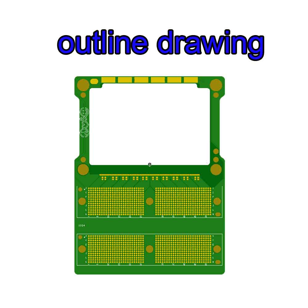
    Arbitrary interconnect PCBs (typically referring to PCBs with flexible routing capabilities) are widely used in various electronic products due to their advantages in flexible routing and high-density integration. Here are some typical application areas:

    Smartphones and Tablets
    In smartphones and other mobile devices, arbitrary interconnect PCBs are used to achieve complex internal connections and support high-density component layouts. This PCB design meets the stringent requirements for performance and miniaturization.

    Computer Motherboards
    Computer motherboards use arbitrary interconnect PCBs to enable complex connections between the processor, memory, storage devices, and other peripheral components. This design provides high data transfer speeds and stable performance.

    Communication Equipment
    In communication equipment such as routers, switches, and base stations, arbitrary interconnect PCBs support high-frequency signal transmission and processing. These PCBs require precise routing and high-frequency performance to ensure signal quality and system stability.

    Medical Devices

    In medical devices such as electrocardiogram (ECG) machines, ultrasound scanners, and monitors, arbitrary interconnect PCBs provide complex circuit connections to ensure high-precision measurements and data processing capabilities.


    Automotive Electronics

    Various electronic systems in modern vehicles, such as infotainment systems, navigation systems, and advanced driver-assistance systems (ADAS), rely on arbitrary interconnect PCBs to handle large amounts of sensor data and control signals. These PCBs need to withstand high temperatures and vibrations.


    Industrial Control Systems

    In industrial automation and control systems, arbitrary interconnect PCBs are used to connect sensors, actuators, and control units. These PCBs manage complex control logic and signal processing tasks.


    Consumer Electronics

    This includes products like televisions, audio systems, and smart home devices, which often require high-density routing to support multiple functions and interfaces. Arbitrary interconnect PCBs provide flexible design solutions for these requirements.


    Military and Aerospace

    Military and aerospace equipment demands high reliability and performance. Arbitrary interconnect PCBs are used in these fields for complex electronic systems, ensuring stable operation in extreme environments.

    These application areas demonstrate the wide applicability and importance of arbitrary interconnect PCBs in meeting the demands of high-density and complex routing requirements.

    Design Challenges of Arbitrary Interconnect PCBs

    Designing arbitrary interconnect PCBs presents several challenges:


    Signal Integrity

    Complex routing can lead to signal issues like interference and delay. Precise signal path management is crucial, especially in high-frequency applications, to ensure signal clarity and stability.


    Electromagnetic Compatibility (EMC)

    Dense routing can cause electromagnetic interference (EMI). Effective shielding, grounding, and filtering are essential to meet EMC standards and minimize interference with other devices.


    Thermal Management

    High-density designs may lead to heat buildup between components. Proper thermal distribution and cooling solutions, such as heat sinks, are necessary to prevent overheating and ensure circuit performance.


    Routing Complexity

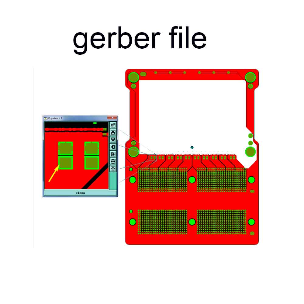
    Managing intricate connections and layer crossings adds difficulty to design and manufacturing. Clear and reliable routing is needed to avoid short circuits and production issues.
    gerber file4x1

    Layer Stack-Up Design

    Multi-layer PCBs require precise control of layer insulation, copper thickness, and alignment to ensure proper electrical isolation and mechanical stability.


    Manufacturing Tolerances

    High-density PCBs demand strict manufacturing tolerances. Any minor deviations can affect functionality, so design must account for production capabilities and tolerances.


    Cost Control

    Complex designs often increase material, processing, and testing costs. Balancing performance requirements with budget constraints is crucial.


    Testing and Debugging

    Complex routing complicates testing and debugging. Design-for-testability (DFT) techniques help simplify these processes.

    These challenges require experienced designers and advanced tools to ensure high-performance and reliable arbitrary interconnect PCBs.

    Unveiling the Power of High-Density Interconnect PCB Technology
    Engineering Issue Confirmationtt7

    In the rapidly advancing world of electronics, High-Density Interconnect PCB (HDI PCB) technology stands out as a game-changer. HDI PCB Manufacturing has revolutionized how complex electronic systems are designed and produced, offering unparalleled benefits in terms of performance and efficiency.


    Understanding HDI Technology

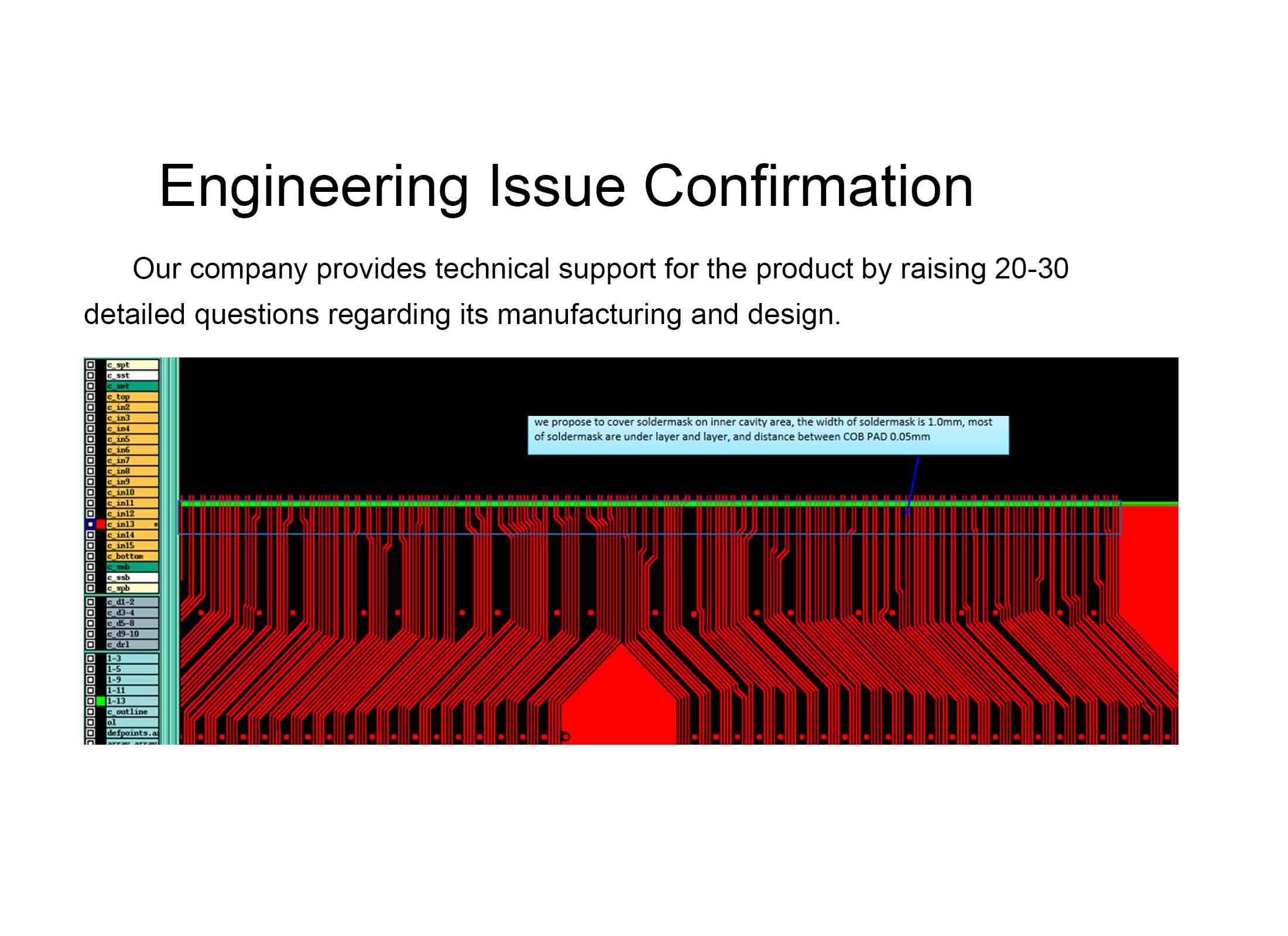
    HDI Board Design focuses on enhancing the interconnectivity of electronic components. The HDI Technology involves advanced techniques like microvias and blind/buried vias, which allow for more complex circuit designs and improved signal integrity. This technology supports High-Density Interconnect Technology, enabling the creation of compact, high-performance circuit boards.


    Key Features and Benefits

    HDI PCB Features include increased component density, improved electrical performance, and reduced board size. The Advanced HDI PCB design integrates these features, providing significant HDI PCB Benefits such as enhanced reliability and better thermal management. HDI Circuit Boards are designed to handle high-speed signals with minimal interference, making them ideal for cutting-edge applications.


    Manufacturing and Process

    The HDI PCB Process involves several critical steps, including precision drilling for microvias and meticulous layer stacking. HDI PCB Fabrication requires advanced equipment and expertise to ensure high-quality results. Microvias in HDI PCBs play a crucial role in connecting different layers within the PCB, contributing to the overall functionality and reliability of the board.


    Applications and Capabilities

    HDI PCB Applications span various industries, including telecommunications, automotive, and medical devices. The HDI PCB Capabilities allow for the integration of complex circuits in smaller form factors, making them suitable for modern electronic devices that demand high performance and compact size.


    In summary, HDI PCB technology represents a significant leap forward in the field of electronics, offering superior performance, reliability, and design flexibility. As HDI PCB Manufacturing continues to evolve, it paves the way for more advanced and efficient electronic solutions.