


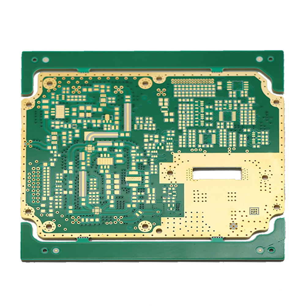


Optical Module HDI PCB Optical Module Gold Finger PCB


Product manufacturing instructions
| Type | two layer HDI,impedance,resin plug hole |
| Materia | Panasonic M6 Copper-Clad Laminate |
| Number of layer | 10L |
| Board Thickness | 1.2mm |
| Single size | 150*120mm/1SET |
| Surface finish | ENEPIG |
| Inner copper thickness | 18um |
| Outer copper thickness | 18um |
| Color of solder mask | green(GTS,GBS) |
| Silkscreen color | white(GTO,GBO) |
| Via treatment | 0.2mm |
| Density of mechanical drilling hole | 16W/㎡ |
| Density of laser drilling hole | 100W/㎡ |
| Min via size | 0.1mm |
| Min line width/space | 3/3mil |
| Aperture ratio | 9mil |
| Pressing times | 3 time |
| Drilling times | 5time |
| PN | E240902A |
Key Control Points in the Production of
Optical Module HDI Gold Finger PCBs

- 1、Precision Etching Control The wiring of gold fingers and HDI PCBs is highly intricate, making the control of the etching process particularly important. Poor etching can lead to uneven line widths, short circuits, or open circuits. Therefore, high-precision etching equipment must be used, and regular calibration is necessary to ensure accuracy and consistency in the etching process.
3、Lamination Process Control Lamination is a critical step where multiple PCB layers are pressed together. Controlling the temperature, pressure, and time during lamination is crucial to ensure the firm bonding of layers and uniform board thickness. Poor lamination can result in delamination or voids, affecting both electrical performance and mechanical strength.
4、Gold Finger Plating Thickness Control The thickness of the gold plating on the gold fingers directly affects insertion life and contact reliability. If the gold plating is too thin, it may wear out quickly; if too thick, it increases costs. Therefore, during the plating process, gold plating time and current density must be strictly controlled to ensure the plating thickness meets the standards (typically 30-50 microinches).
5、Impedance Control and Testing Optical module HDI PCBs often
handle high-speed signals, making impedance control crucial. During
production, impedance testing equipment should be used to monitor and
measure critical signal traces in real-time, ensuring that the impedance
is within the design range (e.g., 100 ohms). Non-compliant impedance can
cause signal integrity issues, such as reflections and crosstalk.
6、Soldering Quality Control Due to the high density of components
involved in optical module PCBs, the soldering process must be highly
precise. Advanced reflow soldering and wave soldering equipment are
required, and soldering temperature profiles must be strictly controlled
to ensure the robustness of solder joints and the reliability of
electrical connections.
7、Surface Cleaning and Protection At every stage of production, the PCB surface must be kept clean to avoid dust, fingerprints, or oxidation residues. These contaminants can cause electrical shorts or affect the quality of the plating. After production, appropriate protective coatings should be applied to prevent moisture and contaminants from penetrating.
8、Quality Inspection and Verification Comprehensive quality inspections, including visual inspection, electrical testing, and functional testing, are essential. Common inspection methods include Automated Optical Inspection (AOI), flying probe testing, and X-ray inspection to ensure that each PCB meets design specifications and quality standards.
The Importance of Routing in Optical
Module HDI PCBs
- Dimensions and Spacing: The width and spacing of the gold fingers need to be strictly controlled to ensure a perfect fit with the connectors. Generally, the width of the gold fingers is 0.5mm, with a spacing of 0.5mm.
-
Edge Chamfering: Chamfering is usually required on the edges
of the PCB where the gold fingers are located to facilitate smoother
insertion into slots.
Layer Count and Stacking: HDI PCBs usually include multilayer designs to provide more electrical connection options. The layer count and stacking design need to be considered to ensure both signal integrity and power integrity.
Microvias: Utilizing microvia technology, such as blind and buried vias, can effectively reduce the length of interlayer connections, thereby reducing signal delay and loss. These microvias require precise control of their position and dimensions.
Routing Density: Due to the high routing density of HDI boards, special attention must be paid to the width and spacing of traces. Typically, trace widths are 3-4 mil, and spacing is also 3-4 mil.

3、Signal Integrity
Differential Pair Routing: High-speed signal transmission commonly used in optical modules requires differential pair routing to reduce electromagnetic interference and signal reflection. The length and spacing of differential pairs need to match, ensuring impedance control within a reasonable range (e.g., 100 ohms).
Impedance Control: In high-speed signal routing, strict impedance control is essential. Impedance matching can be achieved by adjusting trace width, spacing, and layer stacking.
Via Usage: The use of vias should be minimized, as they introduce parasitic capacitance and inductance, affecting signal quality. When necessary, appropriate via types (such as blind and buried vias) and locations should be chosen.
Decoupling Capacitors: Proper placement of decoupling capacitors helps stabilize the power supply voltage and reduce power noise.
Power Plane Design: Adopting solid power plane designs ensures uniform current distribution and reduces electromagnetic interference (EMI).
Thermal Management: Since optical modules generate significant heat during operation, thermal management solutions should be considered in the design, such as using thermal vias, conductive materials, or heat sinks to enhance heat dissipation efficiency.
6、Material Selection
Substrate Material: Choose substrates suitable for high-frequency applications, such as polyimide (PI) or fluoropolymers, to ensure reliable and stable signal transmission.
Solder Mask: Use high-temperature, low-loss solder mask materials to ensure the protection of the traces and electrical performance.
Gold finger HDI PCBs are widely used across
various fields due to their high density and high-performance characteristics:

5、Medical Devices: In high-demand medical equipment like CT scanners, MRI machines, and other diagnostic tools, gold finger HDI PCBs ensure accurate data transmission and reliable operation of the equipment.
- 6、Aerospace: These PCBs are used in the control systems of satellites, aircraft, and spacecraft, as they can withstand harsh environmental conditions while maintaining high performance.
- 7、Industrial Control: In the field of industrial automation, PLCs (Programmable Logic Controllers), and industrial robots, gold finger HDI PCBs provide reliable control and signal transmission.
Gold finger
Detailed Introduction to Gold Fingers
Gold fingers refer to the gold-plated areas on the edge of a printed circuit board (PCB). They are typically used to make electrical connections with connectors. The name "gold finger" comes from their appearance: the strip-like gold-plated sections resemble fingers. Gold fingers are commonly used in insertable PCBs, such as memory sticks, graphics cards, and other devices, to connect with slots. The primary function of gold fingers is to provide reliable electrical connections through a highly conductive gold plating layer while ensuring wear resistance and corrosion resistance.
Classification of Gold Fingers
Gold fingers can be classified based on their function, position, and manufacturing process:
Electrical Connection Gold Fingers: These gold fingers are mainly used to provide stable electrical connections, such as in memory sticks, graphics cards, and other plug-in modules. They transmit electrical signals by being inserted into slots on the motherboard or other devices.
Power Supply Gold Fingers: These are used to provide power or grounding connections, ensuring that devices receive stable power input.

2、Based on Position:
Edge Gold Fingers: Typically located at the edge of the PCB, they are used for slot connections and are commonly found in memory sticks, graphics cards, and communication modules. This is the most common type of gold finger.
Non-Edge Gold Fingers: These gold fingers are not located at the edge of the PCB but are positioned internally for specific connections or functions, such as test points or internal module connections.
3、Based on Manufacturing Process:
Immersion Gold Fingers: These are created using a chemical deposition process to apply a layer of gold onto the copper foil. They have a smooth, fine surface but a thinner gold layer, typically used for lower-frequency electrical connections.
Electroplated Gold Fingers: Made using an electroplating process, these gold fingers have a thicker gold layer and are more wear-resistant, suitable for high-reliability electrical connections requiring frequent insertion and removal, such as in memory sticks and graphics cards. This process typically uses a gold layer thickness of 30-50 microinches to ensure durability and good conductivity.
4、Based on Connection Method:
Straight Insert Gold Fingers: Directly inserted into the slot, the slot's elasticity grips the gold fingers. This method is widely used in memory sticks and graphics cards.
Latch Gold Fingers: Connected using latches or other fastening devices, providing additional mechanical fixation, commonly used for larger modules and applications requiring more stable connections.
Application Characteristics of Gold Fingers
- High Conductivity and Stability: The main material of gold fingers is gold plating, which has excellent and stable conductivity, providing superior electrical performance.
- Wear Resistance: Applications involving frequent insertion and removal require gold fingers to have good wear resistance. The gold plating layer offers this protection, ensuring that gold fingers do not wear out or oxidize easily during use.
- Corrosion Resistance: The gold plating layer on gold fingers not only provides conductivity but also resists corrosive substances in the environment, extending the lifespan of the gold fingers.
Classification of Optical Modules

1、Based on Transmission Speed:
10G Optical Modules: Used for 10 Gigabit Ethernet applications.
25G Optical Modules: Designed for 25 Gigabit Ethernet.
40G Optical Modules: Used in 40 Gigabit Ethernet networks.
100G Optical Modules: Suitable for 100 Gigabit Ethernet networks.
400G Optical Modules: For ultra-high-speed 400 Gigabit Ethernet applications.
2、Based on Transmission Distance:
Short-Range Optical Modules (SR): Typically support distances up to 300 meters using multimode fiber (MMF).
Long-Range Optical Modules (LR): Designed for distances up to 10 kilometers using single-mode fiber (SMF).
Extended Range Optical Modules (ER): Can transmit up to 40 kilometers over SMF.
Very Long-Range Optical Modules (ZR): Support distances greater than 80 kilometers over SMF.
3、Based on Wavelength:
850nm Modules: Generally used for short-range transmission over multimode fiber.
1310nm Modules: Suitable for medium-range transmission over single-mode fiber.
1550nm Modules: Used for long-range transmission, particularly over single-mode fiber.
4、Based on Form Factor:
SFP (Small Form-Factor Pluggable): Commonly used for 1G and 10G networks.
SFP+ (Enhanced Small Form-Factor Pluggable): Used for 10G networks with higher performance.
QSFP (Quad Small Form-Factor Pluggable): Suitable for 40G applications.
QSFP28: Designed for 100G networks, offering a higher density solution.
CFP (C Form-Factor Pluggable): Used in 100G and 400G applications, larger than SFP/QSFP modules.
5、Based on Application:
Data Center Optical Modules: Designed for high-speed data transmission within data centers.
Telecom Optical Modules: Used in telecommunications infrastructure for long-distance data transmission.
Industrial Optical Modules: Built for rugged environments, with high resistance to temperature variations and electromagnetic interference.
How to Distinguish HDI Step Counts
Buried Vias: Holes embedded within the board, not visible from the outside.
Blind Vias: Holes that are visible from the outside but not see-through.
Step Count: The number of different types of blind vias, as viewed from one end of the board, can be defined as the step count.
Lamination Count: The number of times blind/buried vias pass through multiple cores or dielectric layers.
The PCB is manufactured using Panasonic M6
copper-clad laminate
The PCB is manufactured using Panasonic M6 copper-clad laminate. We have extensive experience in this field and know how to fully utilize the performance of Panasonic M6 materials by focusing on the following areas:
1. Material Selection and Inspection
Strict Supplier Selection: Choose reputable and reliable Panasonic M6 copper-clad laminate suppliers to ensure stable and standard-compliant materials. This can be done by evaluating the supplier's qualifications, production capacity, and quality control systems. Our years of experience have enabled us to establish long-term, stable partnerships with high-quality suppliers, ensuring material quality from the source.
Material Inspection: Upon receiving the copper-clad laminate materials, conduct rigorous inspections to check for defects like damage or stains and to measure parameters such as thickness and dimensions to ensure they meet the requirements. Specialized testing equipment can also be used to test the material's electrical properties, thermal conductivity, and other performance indicators to ensure they meet design requirements. Our professional testing team uses advanced equipment and strict processes to ensure that no detail is overlooked.

2. Design Optimization
Circuit Layout Design: Based on the characteristics of Panasonic M6 copper-clad laminate, design the circuit board layout appropriately. For high-frequency circuits, shorten signal paths to reduce signal reflection and interference. For high-power circuits, fully consider heat dissipation issues, arrange heating elements, and heat dissipation channels properly to maximize the thermal conductivity of the copper-clad laminate. Our design team understands the properties of Panasonic M6 laminate and can precisely layout designs according to various circuit needs.
Stack-Up Design: Optimize the circuit board's stack-up structure based on the circuit's complexity and performance requirements. Choose the appropriate number of layers, interlayer spacing, and insulation materials to ensure signal integrity and electrical performance stability. Also, consider heat transfer and dissipation effects between layers to avoid local overheating. Through extensive practice and continuous optimization, we have developed a scientific and reasonable stack-up design solution.
3. Manufacturing Process Control
Etching Process: Accurately control etching parameters to ensure the precision and quality of the circuit board's traces. Choose suitable etchants and etching conditions to avoid over-etching or under-etching. Additionally, be mindful of environmental protection during the etching process to prevent contamination of the copper-clad laminate. We have rich experience in etching processes and can precisely control the process to ensure the quality of the circuit board.
Drilling Process: Use high-precision drilling equipment and control drilling parameters to ensure hole size and positional accuracy. Care should be taken to avoid damaging the copper-clad laminate, which could affect its performance. Our advanced drilling equipment and skilled operators ensure the accuracy of the drilling process.
Lamination Process: Strictly control lamination parameters to ensure interlayer adhesion and electrical performance. Choose appropriate lamination temperature, pressure, and time to ensure good bonding between the copper-clad laminate and other insulating materials. Also, pay attention to exhaust issues during the lamination process to avoid bubbles and delamination. Our stringent control of the lamination process ensures stable performance of the circuit board.
4. Quality Testing and Debugging
Electrical Performance Testing: Use specialized testing equipment to test the electrical properties of the circuit board, including resistance, capacitance, inductance, insulation resistance, and signal transmission speed. Ensure that the electrical performance meets design requirements and that the low dielectric constant and low dielectric loss tangent characteristics of Panasonic M6 copper-clad laminate are fully utilized. Our advanced and comprehensive testing equipment can test all aspects of the circuit board's electrical performance.
Thermal Performance Testing: Use thermal imaging devices to monitor the working temperature of the circuit board and check the effectiveness of heat dissipation. Perform thermal shock tests to assess the stability of the circuit board's performance under different temperature conditions. Our strict thermal performance testing ensures the stability of the circuit board in various working environments.
Debugging and Optimization: After completing the circuit board manufacturing, perform debugging and optimization. Adjust circuit parameters based on test results to improve the performance and stability of the circuit board. Additionally, constantly summarize experiences and lessons learned to continually improve manufacturing processes and design solutions to better utilize the advantages of Panasonic M6 copper-clad laminate. Our debugging and optimization team can quickly and accurately carry out debugging to continuously improve product quality.
In summary, with our extensive production experience and deep understanding of Panasonic M6 copper-clad laminate materials, we are confident in providing our customers with high-quality PCB products.