

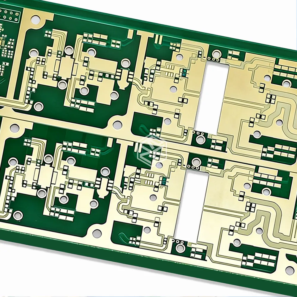
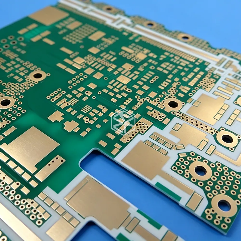
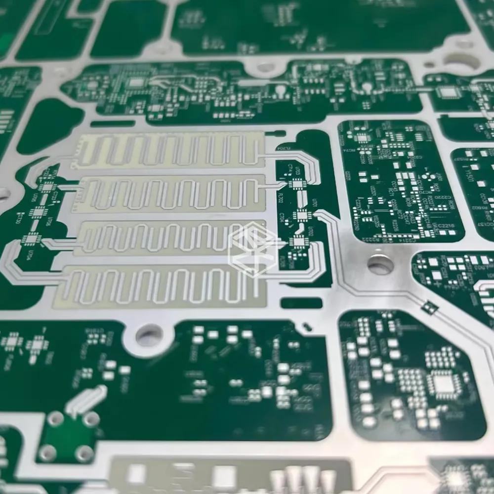






RF PCB Balun Design: Unbalanced-to-Balanced Conversion Dominated by Copper Foil Thickness Tolerance
1. The Tolerance That Breaks Balance
A balun — balanced-to-unbalanced transformer — is one of the most critical passive components in RF and microwave circuit design. It converts a single-ended signal to a differential pair (or vice versa), providing the interface between unbalanced transmission lines (50Ω coax, microstrip) and balanced circuits (mixers, push-pull amplifiers, differential ADCs, antenna feeds).
In a PCB implementation, the balun is typically realized as a coupled-line structure — a Marchand balun, a transformer balun, or a variations thereof. The performance of these structures depends on the precise geometry of coupled transmission lines: line width, line spacing, and crucially, copper foil thickness.
The manufacturing reality: Standard PCB copper foil thickness is specified with a tolerance of approximately ±10%. For 1 oz (35μm) copper, this means the actual thickness can range from 31.5μm to 38.5μm. For ½ oz (17.5μm) copper, the range is 15.75μm to 19.25μm.
This ±10% variation in copper thickness directly translates into variation in characteristic impedance, coupling coefficient, and ultimately, amplitude and phase balance of the balun. The effect is so pronounced that copper thickness tolerance often dominates the unbalanced-to-balanced conversion performance — surpassing the impact of dielectric thickness variation, line width etching tolerance, or material Dk variation.
This article examines why copper foil thickness tolerance is the primary driver of balun performance variation, quantifies the impact on impedance and balance, and provides design strategies for achieving consistent unbalanced-to-balanced conversion in volume production.
2. The Balun: Structure and Sensitivity
2.1 The Marchand Balun — A Coupled-Line Structure
The Marchand balun is the most common PCB-integrated balun topology. It consists of two coupled transmission lines — typically quarter-wave (λ/4) sections — that provide a 180° phase shift between the balanced outputs while transforming the impedance from the unbalanced port.
The operation of the Marchand balun depends on the even-mode and odd-mode impedances of the coupled lines:
- Even-mode impedance (Z₀ₑ): The impedance when both lines are driven with equal-phase signals
- Odd-mode impedance (Z₀ₒ): The impedance when the lines are driven with opposite-phase signals
The characteristic impedance of each line and the coupling coefficient between them are determined by:
Z₀ = √(Z₀ₑ × Z₀ₒ)
The coupling coefficient k is:
k = (Z₀ₑ − Z₀ₒ) / (Z₀ₑ + Z₀ₒ)
Both Z₀ₑ and Z₀ₒ are exquisitely sensitive to the physical geometry of the coupled lines — line width, line spacing, dielectric thickness, and copper thickness.
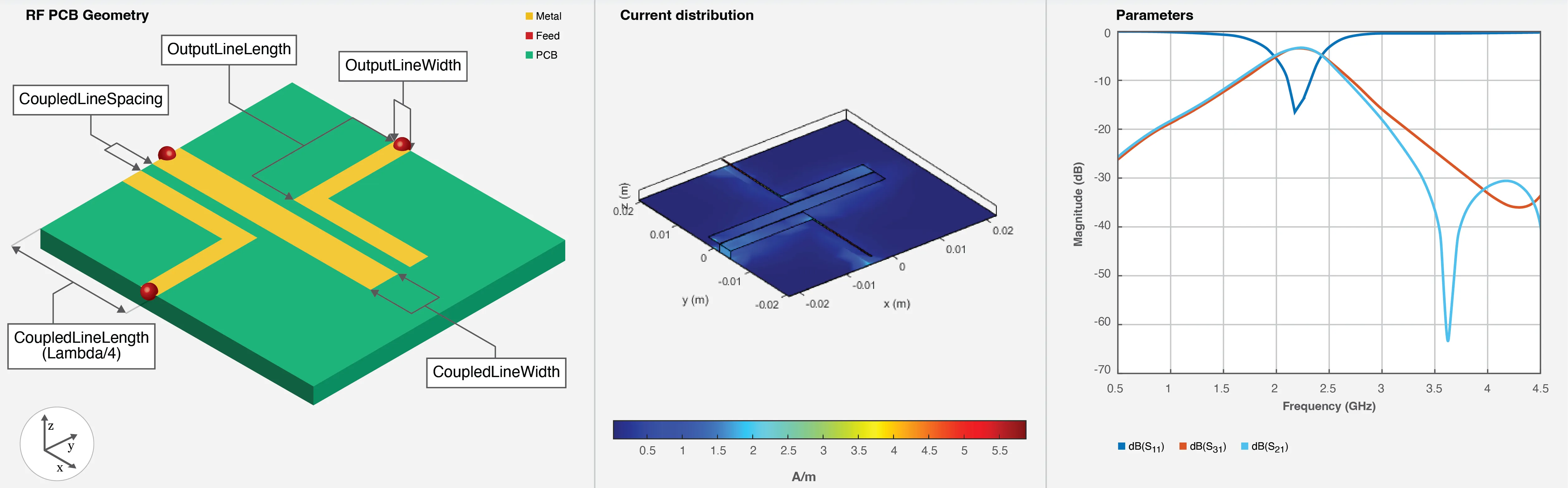
2.2 Why Copper Thickness Matters So Much
In a coupled-line structure, copper thickness affects performance through three mechanisms:
Conductor cross-section: The cross-sectional area of the trace determines its DC resistance and, more importantly, its characteristic impedance. A thicker trace has lower resistance and slightly different field distribution, shifting Z₀.
Fringing capacitance: The fringing fields at the edges of the trace are affected by the trace height. A thicker trace creates more fringing capacitance to the ground plane and to adjacent traces, altering both Z₀ₑ and Z₀ₒ.
Coupling coefficient: The coupling between adjacent lines depends on the spacing between them relative to the trace height. For a fixed line spacing, thicker traces increase the coupling coefficient because the sidewalls of the traces are closer (electrically) to each other.
Table 1 — Sensitivity of coupled-line parameters to copper thickness variation
| Parameter | Effect of +10% Copper Thickness | Effect of -10% Copper Thickness |
|---|---|---|
| Trace cross-section | Increases by 10% | Decreases by 10% |
| Characteristic impedance (Z₀) | Decreases by ~2-3% | Increases by ~2-3% |
| Even-mode impedance (Z₀ₑ) | Decreases | Increases |
| Odd-mode impedance (Z₀ₒ) | Decreases (more coupling) | Increases (less coupling) |
| Coupling coefficient (k) | Increases | Decreases |
The impact is asymmetric: the odd-mode impedance (which depends more on the coupling between adjacent lines) is more sensitive to copper thickness than the even-mode impedance (which depends more on the ground plane spacing).
3. How Copper Thickness Tolerance Destroys Balance
3.1 The Balance Metrics
A balun's unbalanced-to-balanced conversion quality is measured by two metrics:
- Amplitude balance: The difference in magnitude between the two balanced outputs (typically specified as <0.5 dB for good designs)
- Phase balance: The deviation from 180° phase difference between the two balanced outputs (typically specified as <5° for good designs)
When the coupled lines are perfectly symmetric and fabricated to nominal dimensions, the balun achieves excellent amplitude and phase balance. When copper thickness varies from the nominal value, both outputs are affected asymmetrically — because the coupling coefficient changes, and the impedance transformation ratio shifts.
3.2 The Coupling Coefficient Shift
The coupling coefficient k is the most sensitive parameter to copper thickness variation. For a typical edge-coupled microstrip Marchand balun with 4 mil (100μm) line width, 4 mil spacing, and ½ oz copper:
| Copper Thickness | Coupling Coefficient (k) | Amplitude Balance | Phase Balance |
|---|---|---|---|
| Nominal (17.5μm) | 0.45 (design target) | 0.2 dB | 2° |
| +10% (19.25μm) | 0.48 (+6.7%) | 0.5 dB | 5° |
| -10% (15.75μm) | 0.42 (-6.7%) | 0.6 dB | 6° |
A ±6.7% variation in coupling coefficient translates to amplitude balance degradation of 0.3-0.4 dB and phase balance degradation of 3-4° — simply from copper thickness tolerance alone.
For high-performance applications requiring <0.5 dB amplitude balance and <3° phase balance, this variation can push the balun out of specification on a significant fraction of production boards.
3.3 The Impedance Transformation Shift
The Marchand balun provides impedance transformation in addition to balanced-to-unbalanced conversion. The transformation ratio depends on the ratio of Z₀ₑ to Z₀ₒ.
When copper thickness varies, both Z₀ₑ and Z₀ₒ shift — but not proportionally. The odd-mode impedance (which depends on coupling between lines) shifts more than the even-mode impedance (which depends on ground plane spacing). This differential shift changes the impedance transformation ratio, degrading the match at the unbalanced port.
The result: increased return loss at the input, reduced power transfer to the balanced outputs, and degraded system performance.
Table 2 — Impact of copper thickness variation on balun performance
| Parameter | Nominal (17.5μm) | +10% Copper | -10% Copper |
|---|---|---|---|
| Z₀ₑ (Ω) | 85 | 83 (-2.4%) | 87 (+2.4%) |
| Z₀ₒ (Ω) | 45 | 42 (-6.7%) | 48 (+6.7%) |
| Z₀ (√Z₀ₑ×Z₀ₒ) (Ω) | 61.8 | 59.0 (-4.5%) | 64.6 (+4.5%) |
| Coupling coefficient k | 0.307 | 0.328 (+6.8%) | 0.289 (-5.9%) |
| Amplitude balance (dB) | 0.10 | 0.45 | 0.55 |
| Phase balance (°) | 1.2 | 4.8 | 5.6 |
Data based on electromagnetic simulation of a typical edge-coupled microstrip Marchand balun on 0.8mm RO4350B substrate, 4 mil line width, 4 mil spacing.
4. Why Copper Thickness Dominates Over Other Tolerances
4.1 Comparison of Manufacturing Tolerances
In PCB manufacturing, multiple parameters vary from board to board and from panel to panel:
| Parameter | Typical Tolerance | Impact on Balun Balance |
|---|---|---|
| Copper thickness | ±10% | High (directly affects Z₀ₑ, Z₀ₒ, k) |
| Line width (etching) | ±10% | Moderate (affects Z₀ but less than copper thickness for coupled structures) |
| Dielectric thickness | ±8-10% | Moderate (affects Z₀ₑ more than Z₀ₒ) |
| Dielectric constant (Dk) | ±2-5% | Low-Moderate (affects phase velocity, not balance directly) |
| Layer registration | ±2-4 mil | Low for edge-coupled (affects broadside-coupled more) |
Why copper thickness dominates: In a coupled-line balun, the odd-mode impedance (Z₀ₒ) — which determines the coupling and thus the balance — is primarily determined by the geometry between the two coupled traces. Copper thickness directly changes the sidewall area and fringing capacitance between adjacent traces. No other tolerance has such a direct, first-order effect on the coupling mechanism.
4.2 The Frequency Scaling Effect
The impact of copper thickness tolerance scales with frequency. At lower frequencies (<1 GHz), the electrical length of the coupled lines is long relative to the physical dimensions, and the balun is more forgiving. At higher frequencies (>5 GHz), the coupled lines are shorter, and any geometry variation has a proportionally larger impact on phase and amplitude balance.
For millimeter-wave applications (>30 GHz), the copper thickness tolerance effect becomes critical. A ±10% copper thickness variation can shift the balun's center frequency by several hundred MHz and degrade balance beyond acceptable limits.
5. Design Strategies for Copper-Thickness-Tolerant Baluns
5.1 Specify Tighter Copper Thickness Tolerance
The most direct approach: specify tighter copper thickness tolerance on your fabrication drawing.
| Application | Standard Tolerance | Recommended RF Tolerance |
|---|---|---|
| General purpose | ±10% | N/A |
| RF (<3 GHz) | ±10% | ±8% |
| RF (3-10 GHz) | ±10% | ±5% |
| Millimeter-wave (>10 GHz) | ±10% | ±3% |
Specify the requirement clearly:
"Copper foil thickness: 17.5μm ±1.0μm (½ oz) for all RF layers. Thickness verification required per IPC-TM-650 2.2.13."
5.2 Use Thinner Copper
Thinner copper has two advantages for balun design:
- Lower percentage variation for the same absolute tolerance (a ±1μm variation on 12μm copper is ±8.3%, vs. ±5.7% on 17.5μm copper)
- Less fringing capacitance from trace edges, reducing the sensitivity of Z₀ₒ to thickness variation
For balun designs, ½ oz (17.5μm) copper is recommended over 1 oz (35μm). For millimeter-wave applications, ⅓ oz (12μm) or even ¼ oz (9μm) copper provides the best thickness control.
5.3 Design for Manufacturing (DFM) — Tolerance-Aware Simulation
Incorporate manufacturing tolerances into your electromagnetic simulations:
- Run Monte Carlo simulations with copper thickness varied by ±10%
- Evaluate worst-case amplitude and phase balance at the tolerance extremes
- If the design fails at worst-case tolerance, either tighten the specification or redesign with larger geometry margins
Simulations that assume nominal copper thickness will overestimate balun performance. Tolerance-aware simulation is essential for production-ready designs.
5.4 Broadside-Coupled vs. Edge-Coupled
Broadside-coupled baluns (where the coupled lines are on adjacent layers) have different sensitivity to copper thickness than edge-coupled baluns. In broadside-coupled structures, the coupling is determined by the dielectric thickness between layers, not by the copper thickness. Copper thickness variation has a smaller impact on the coupling coefficient.
Design trade-off: Broadside-coupled baluns require tight layer registration (typically ±1-2 mil) but are less sensitive to copper thickness. Edge-coupled baluns are easier to fabricate (single-layer) but more sensitive to copper thickness.
For applications where copper thickness control is challenging, consider a broadside-coupled or stripline balun topology.
5.5 Include Balun Test Coupons
Include dedicated balun test coupons on the production panel — a separate balun structure with the same geometry as the design. Measure:
- S-parameters (S11, S21, S31) using a VNA
- Amplitude balance (|S21| vs. |S31|)
- Phase balance (∠S21 vs. ∠S31)
Compare measured values against simulation to verify that the copper thickness achieved the target performance. Reject panels where balance exceeds the specification limit.
6. The Tolerance That Determines Balance
The unbalanced-to-balanced conversion performance of a PCB balun is dominated by copper foil thickness tolerance. Not dielectric variation. Not line width etching tolerance. Not material Dk variation. Copper thickness.
The key takeaways:
- Copper thickness tolerance of ±10% is standard in PCB manufacturing
- This ±10% variation shifts the coupling coefficient by ±6-7% in a typical edge-coupled Marchand balun
- Amplitude balance degrades by 0.3-0.4 dB and phase balance degrades by 3-4° from copper thickness variation alone
- Copper thickness dominates over dielectric thickness, line width, and Dk variation for balun balance
- The effect scales with frequency — millimeter-wave baluns are most sensitive
- Specify tighter tolerance (±5% or better) for RF balun layers
- Use thinner copper (½ oz or ⅓ oz) to reduce the impact
- Run tolerance-aware simulations — Monte Carlo analysis with ±10% copper thickness
- Consider broadside-coupled topologies if copper thickness control is limited
A PCB balun designed with tight copper thickness control — specified, verified, and simulated with tolerance — will achieve the amplitude and phase balance that your RF system requires. A design that ignores copper thickness tolerance may measure 0.5 dB imbalanced and 5° out of phase — the difference between a working differential interface and one that fails.
7. Frequently Asked Questions
Q1: Why does copper foil thickness affect balun performance?
A: Copper thickness directly affects the cross-sectional geometry of coupled transmission lines. In a Marchand balun, the odd-mode impedance (which determines coupling) is particularly sensitive to the sidewall area and fringing capacitance between adjacent traces — both of which change with copper thickness.
Q2: What is the standard copper thickness tolerance in PCB manufacturing?
A: Standard PCB manufacturing specifies copper foil thickness with a tolerance of approximately ±10%. For 1 oz (35μm) copper, this means 31.5–38.5μm. For ½ oz (17.5μm), this means 15.75–19.25μm.
Q3: How much does ±10% copper thickness affect balun balance?
A: A ±10% copper thickness variation shifts the coupling coefficient by ±6-7%, degrading amplitude balance by 0.3-0.4 dB and phase balance by 3-4° in a typical edge-coupled Marchand balun.
Q4: Why does copper thickness dominate over other tolerances for baluns?
A: In a coupled-line balun, the odd-mode impedance (Z₀ₒ) — which determines the coupling and thus the balance — is primarily determined by the geometry between the two coupled traces. Copper thickness directly changes the sidewall area and fringing capacitance. No other tolerance has such a direct, first-order effect on the coupling mechanism.
Q5: What copper thickness should I specify for RF balun designs?
A: For RF balun designs, specify ½ oz (17.5μm) copper with ±5% tolerance for designs above 3 GHz. For millimeter-wave applications (>30 GHz), consider ⅓ oz (12μm) or ¼ oz (9μm) copper with ±3% tolerance.
Q6: What is the difference between amplitude balance and phase balance?
A: Amplitude balance is the difference in magnitude (dB) between the two balanced outputs. Phase balance is the deviation from 180° phase difference. Typical specifications are <0.5 dB amplitude balance and <5° phase balance for good balun designs.
Q7: Does the impact of copper thickness scale with frequency?
A: Yes. At higher frequencies, the coupled lines are electrically longer relative to physical dimensions, and any geometry variation has a proportionally larger impact on phase and amplitude balance. Millimeter-wave baluns (>30 GHz) are most sensitive.
Q8: What is the difference between edge-coupled and broadside-coupled baluns for copper thickness sensitivity?
A: Edge-coupled baluns (coupled lines on the same layer) are more sensitive to copper thickness because coupling depends on the sidewall area between adjacent traces. Broadside-coupled baluns (coupled lines on adjacent layers) are less sensitive to copper thickness because coupling is determined by the dielectric thickness between layers.
Q9: How can I verify that my balun meets specifications after fabrication?
A: Include dedicated balun test coupons on the production panel. Measure S-parameters (S11, S21, S31) using a VNA. Calculate amplitude balance (|S21| vs. |S31|) and phase balance (∠S21 vs. ∠S31). Compare against simulation and specification limits.
Q10: Should I run simulations with copper thickness tolerance included?
A: Yes. Run Monte Carlo simulations with copper thickness varied by ±10%. Evaluate worst-case amplitude and phase balance at the tolerance extremes. If the design fails at worst-case tolerance, either tighten the specification or redesign with larger geometry margins.
8. About Richfulljoy
Richfulljoy specializes in high-precision RF and microwave PCB manufacturing with tight copper foil thickness control for baluns, couplers, filters, and impedance-controlled structures.









