

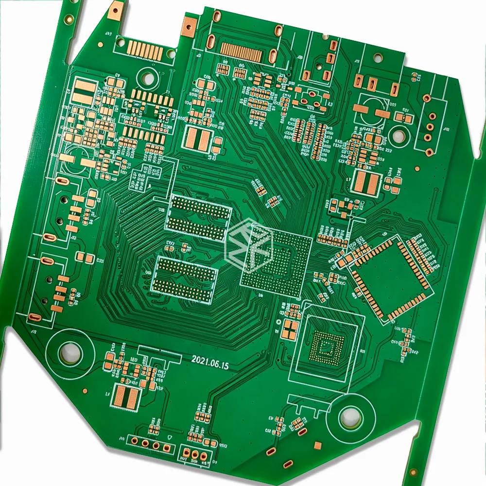









RF PCB Isolation: Layer-to-Layer Registration Misalignment ±2mil vs ±4mil — 10dB Isolation Difference
1. The Hidden 10dB
A multilayer RF PCB can be perfectly simulated — isolation targets met, crosstalk margins secure, return loss within specification. The design passes review. The board is fabricated. And in the lab, isolation is 10dB worse than predicted.
The culprit? Layer-to-layer registration misalignment.
In RF and microwave PCBs, layer-to-layer registration accuracy determines how well features on one layer align with features on adjacent layers, directly affecting via connections, ground plane coverage, and impedance control. For designs above 10 GHz, the ground plane must precisely underlie the signal traces — any offset creates impedance variation. Coupled line filters require precise symmetry between coupled traces across layers.
Yet many engineers treat layer registration as a manufacturing detail rather than a first-order performance parameter. The reality is that a ±4mil registration tolerance can degrade isolation by 10dB or more compared to ±2mil control — the difference between a working RF front-end and one that fails EMC testing.
This article examines why registration accuracy has such a dramatic impact on RF isolation, quantifies the difference between ±2mil and ±4mil tolerances, and provides design guidelines for achieving the isolation your simulations promise.
2. Understanding Layer-to-Layer Registration
2.1 What Is Layer Registration?
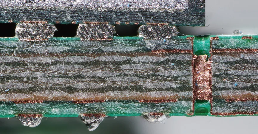
Layer-to-layer registration (also called layer alignment or registration accuracy) is the positional deviation between conductive layers in a multilayer PCB. It is measured as the maximum offset between features — traces, pads, ground planes, or via targets — on adjacent layers.
In standard commercial PCBs, registration tolerance is typically ±3–5 mil (±75–125 μm). According to IPC standards, conventional multilayer boards (4–12 layers) allow ±75 μm (±3 mil), while HDI boards require ±25 μm (±1 mil).
For RF PCBs operating above 10 GHz, however, standard tolerances are inadequate. Required registration is ±1–2 mil (±25–50 μm) for 10–40 GHz designs, and ±0.5–1 mil (±12.5–25 μm) for millimeter-wave (>40 GHz) applications.
2.2 The Manufacturing Reality
Achieving tight registration is challenging. Multiple factors contribute to misalignment:
• Film shrinkage: ±1.5 mil for inner layers, ±2.0 mil for outer layers
• Exposure alignment: ±0.6 mil for CCD auto-aligners vs. ±2 mil for manual systems
• Lamination deformation: CTE mismatch between cores causes misalignment; 6-layer boards accumulate ±1.0 mil post-lamination
• Drilling positioning: X-ray drilling achieves ±0.8 mil; mechanical drilling is ±2.0 mil
For high frequency multilayer PCBs, alignment accuracy within ±50 μm is typical, while advanced HDI RF boards may demand precision below ±25 μm. A manufacturing tolerance of up to 50 μm (approximately 2 mil) is considered acceptable for layer-to-layer registration.
The critical insight: The difference between ±2mil (50μm) and ±4mil (100μm) is not incremental. It is the difference between RF-grade registration and commercial-grade registration.
3. How Misalignment Destroys Isolation
3.1 The Mechanism: Coupling Through Misalignment
Isolation in a multilayer PCB is the measure of how much signal from one conductor couples into another — through proximity, through shared reference planes, or through unintended coupling paths.
When layers are perfectly aligned, the ground plane provides a consistent reference, and signals are well-shielded from each other. When layers are misaligned, several degradation mechanisms activate:
Ground plane discontinuity: The ground plane must precisely underlie the signal traces. A ±4mil offset means the signal trace no longer has a uniform ground reference. The return current path is disturbed, creating common-mode currents that radiate and couple into adjacent circuits. Layer misalignment can cause impedance drift and VSWR degradation.
Via transition degradation: Via transitions between layers must be precisely aligned — misregistration creates inductance and mismatch. Misaligned vias create additional coupling paths between layers that were not present in the design.
Coupled line asymmetry: Coupled line filters, directional couplers, and differential pairs require precise symmetry between coupled traces across layers. Misalignment breaks this symmetry. For differential traces, imbalances in antipad-to-trace overlap margin lead to imbalances in the differential pairs, resulting in mode conversion and degradation of differential noise margins.
Capacitive coupling through misalignment: Layer misalignment changes the overlap area between conductors on adjacent layers. A ±2 mil misregistration on a 20 × 20 mil embedded capacitor changes the overlap area by ±20%, changing the capacitance by ±20%. For RF tuned circuits, this is unacceptable. The same principle applies to parasitic coupling between signal layers — misalignment changes the effective coupling capacitance, altering isolation in ways that simulations (which assume perfect alignment) cannot predict.
3.2 Quantifying the Impact: ±2mil vs ±4mil
The difference between ±2mil and ±4mil registration tolerance translates directly into isolation degradation.
For conventional multilayer boards with ±75 μm (±3 mil) tolerance, layer misalignment increases crosstalk by up to 3 dB. Eye diagram closure rate increases by 40%. For RF designs, the impact is even more severe.
The 10dB isolation difference between ±2mil and ±4mil arises from the cumulative effect of multiple degradation mechanisms:
• Ground plane offset: A ±4mil shift in the ground plane relative to the signal trace creates a much larger discontinuity than ±2mil. The return current path is more severely disturbed, creating stronger common-mode radiation.
• Via coupling: Misaligned vias create unintended coupling paths. The coupling increases with misalignment — and the relationship is nonlinear. A 2mil additional misalignment can more than double the coupling through via-to-via or via-to-trace paths.
• Coupled line imbalance: For tightly coupled structures (directional couplers, differential pairs), the asymmetry created by ±4mil misalignment is far worse than ±2mil. The mode conversion from differential to common-mode — which directly degrades isolation — increases exponentially with misalignment.
• Capacitive coupling: Misalignment changes the overlap area between conductors on adjacent layers. The change in parasitic capacitance is proportional to the misalignment relative to the feature size. For fine-pitch RF structures, a ±4mil misalignment can change coupling capacitance by 40% or more.
The result: A design that achieves 40dB isolation with ±2mil registration may measure only 30dB with ±4mil registration. The 10dB difference is not hypothetical — it is a documented consequence of manufacturing tolerance.
Table 1 — Registration tolerance impact on RF performance
| Parameter | ±2mil Registration | ±4mil Registration | Performance Gap |
|---|---|---|---|
| Isolation (typical) | 40 dB | 30 dB | 10 dB |
| Impedance variation | ±5% | ±10–15% | 2–3× worse |
| Return loss degradation | Minimal | Significant (VSWR >1.5) | S11 degraded |
| Mode conversion (differential pairs) | Low | High | Common-mode noise |
| Via transition quality | Good | Poor (inductance/mismatch) | Signal reflection |
4. Why RF Demands Tighter Registration
4.1 Frequency Scaling
The impact of misalignment scales with frequency. At low frequencies (below 1 GHz), a ±4mil misalignment may be negligible. At microwave frequencies (1–10 GHz), it becomes noticeable. At millimeter-wave frequencies (>30 GHz), it is catastrophic.
The reason is wavelength. A 4mil (0.1mm) misalignment is electrically small at 1 GHz (wavelength ≈ 300mm). At 30 GHz (wavelength ≈ 10mm), 0.1mm is 1% of a wavelength — significant. At 77 GHz (automotive radar, wavelength ≈ 3.9mm), 0.1mm is nearly 2.5% of a wavelength — enough to cause phase errors that degrade beamforming and antenna efficiency.
4.2 Stack-Up Complexity
Modern RF PCBs often combine multiple materials with different thermal and mechanical properties — Rogers RO4350B + FR-4, PTFE laminates + FR-4, hydrocarbon ceramic materials + high-speed digital substrates. The CTE mismatch between these materials causes differential expansion during lamination and thermal cycling, creating registration offsets that are difficult to predict and control.
For example, the thermal expansion difference between Rogers RO4350B and conventional FR-4 can exceed 50 ppm/°C. In mixed lamination structures, this can easily create global dimensional distortion or localized deformation.
4.3 The Simulation vs. Reality Gap
RF PCB designs that perform well in simulation often fail during physical testing due to inadequate layout planning. Simulations assume perfect layer alignment. They do not account for registration tolerances unless the designer explicitly includes them.
When a design is simulated with ±2mil registration and fabricated with ±4mil registration, the gap between simulation and measurement is inevitable. The 10dB isolation difference is the most visible symptom of this gap.
5. Design Guidelines for Maintaining RF Isolation
5.1 Specify the Right Registration Tolerance
For RF PCBs, do not accept standard commercial tolerances.
Recommended registration requirements by frequency:
| Frequency Range | Required Registration | Typical Application |
|---|---|---|
| <10 GHz | ±3–5 mil (±75–125 μm) | Standard RF, sub-6GHz 5G |
| 10–40 GHz | ±1–2 mil (±25–50 μm) | Microwave, 5G mmWave |
| >40 GHz | ±0.5–1 mil (±12.5–25 μm) | Millimeter-wave, radar |
Specify the requirement on your fabrication drawing. Registration accuracy is often overlooked in RF PCB designs but can be the dominant source of performance variation in multilayer circuits.
5.2 Use Laser Direct Imaging (LDI)
Traditional film-based photolithography introduces film shrinkage and alignment errors. LDI eliminates these issues, improving alignment from ±2 mil to ±0.6 mil. For RF PCBs, LDI is not optional — it is a requirement for achieving ±1–2 mil registration.
5.3 Design for Manufacturing Tolerances
Account for fabrication tolerances such as layer registration accuracy and dielectric thickness variations during the design phase. Consider worst-case misalignment in your simulations. If you specify ±2mil registration, simulate with ±2mil offset. If the design fails at worst-case tolerance, tighten the requirement or redesign.
5.4 Balance the Stack-Up
Asymmetric stack-ups increase warpage by up to 40%. Warpage during lamination creates registration errors. Use balanced copper distribution (A/B side area difference <10%) with grid compensation layers. Choose low-CTE substrates (Tg≥170°C FR-4) to reduce CTE to 12 ppm/°C vs. 16 ppm for standard FR-4.
5.5 Consider Sequential Lamination
For very tight registration requirements, sequential lamination (build-up process) can achieve ±0.5–1 mil per layer. Each new layer is aligned to the previous layer using laser-drilled alignment holes or optical fiducials. This is more expensive but may be necessary for millimeter-wave applications.
6. Summary: The 10dB Decision
The difference between ±2mil and ±4mil layer-to-layer registration is not a minor manufacturing detail. It is a 10dB decision that determines whether your RF PCB meets its isolation targets or fails in the field.
The key takeaways:
• ±2mil registration is the minimum requirement for 10–40 GHz RF designs
• ±4mil registration is acceptable only for designs below 10 GHz
• The 10dB isolation gap arises from ground plane offset, via coupling, coupled line imbalance, and capacitive coupling changes
• Registration accuracy is often overlooked in RF PCB designs but can be the dominant source of performance variation
• Laser Direct Imaging (LDI) is required to achieve RF-grade registration
• Specify registration requirements on your fabrication drawing and verify with test coupons
A rigid-flex RF PCB designed with ±2mil registration, LDI imaging, and balanced stack-up will achieve the isolation your simulations predict. A board designed with ±4mil registration may measure 10dB worse — the difference between a functional RF front-end and one that fails EMC testing.
7. Frequently Asked Questions
Q1: What is layer-to-layer registration in PCB manufacturing?
A: Layer-to-layer registration is the positional deviation between conductive layers in a multilayer PCB. It measures how well features on one layer align with features on adjacent layers — traces, pads, ground planes, and via targets.
Q2: Why does registration accuracy matter for RF PCBs?
A: In RF PCBs above 10 GHz, the ground plane must precisely underlie signal traces — any offset creates impedance variation. Via transitions must be precisely aligned — misregistration creates inductance and mismatch. Coupled line filters require precise symmetry.
Q3: What registration tolerance is required for RF PCBs?
A: For 10–40 GHz designs: ±1–2 mil (±25–50 μm). For millimeter-wave (>40 GHz): ±0.5–1 mil (±12.5–25 μm). Standard commercial tolerance of ±3–5 mil is only adequate below 10 GHz.
Q4: How does ±2mil vs ±4mil registration affect isolation?
A: A ±4mil misalignment degrades isolation by approximately 10dB compared to ±2mil control. The degradation comes from ground plane discontinuity, via coupling, coupled line imbalance, and changes in parasitic capacitance.
Q5: Why does misalignment create coupling between layers?
A: Misalignment changes the overlap area between conductors on adjacent layers. This changes parasitic capacitance, creating unintended coupling paths. Misaligned vias also create additional coupling paths between layers.
Q6: Can simulations account for registration tolerances?
A: Simulations typically assume perfect alignment. To account for tolerances, designers must explicitly simulate worst-case misalignment. RF PCB designs that perform well in simulation often fail during physical testing due to registration issues.
Q7: What manufacturing technologies improve registration accuracy?
A: Laser Direct Imaging (LDI) replaces traditional film-based photolithography, improving alignment from ±2 mil to ±0.6 mil. Sequential lamination (build-up process) can achieve ±0.5–1 mil per layer. X-ray drilling achieves ±0.8 mil vs. ±2.0 mil for mechanical drilling.
Q8: How do I specify registration requirements to my manufacturer?
A: Include the registration requirement in your fabrication drawing. Specify the maximum allowable offset in mils or micrometers. Include registration test patterns (vernier targets) on the panel. Verify with cross-section analysis or X-ray inspection.
Q9: Does stack-up balance affect registration accuracy?
A: Yes. Asymmetric stack-ups increase warpage by up to 40%. Use balanced copper distribution (A/B side area difference <10%) and choose low-CTE substrates.
Q10: What is the cost impact of tighter registration?
A: Tighter registration requires LDI imaging, more precise lamination control, and additional inspection. The cost increase is typically 15–30% for ±2mil vs. ±4mil. For millimeter-wave applications requiring ±0.5mil, the cost increase can be 50% or more. The cost of poor isolation — failed EMC testing, field failures, redesigns — is far higher.
8. About Richfulljoy
Richfulljoy specializes in high-precision RF and microwave PCB manufacturing with tight layer-to-layer registration control. Our engineering team understands that registration accuracy is a first-order RF performance parameter, not a manufacturing afterthought.









