








How to identify the invisible defects of PCBA clearly?
X-RAY Inspection Standards
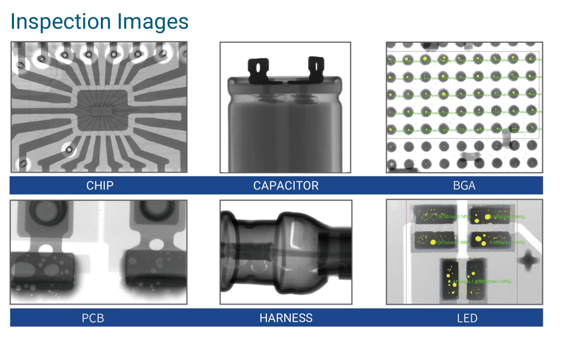
1. BGA solder joints have no offset:
Judgment criteria: acceptable when the offset is less than half of the circumference of the solder pad; When the offset is greater than or equal to half of the circumference of the solder pad, it shall be rejected.
2. BGA solder joints have no short circuit:
Judgment criteria: If there is no tin connection between the solder joints, it is acceptable; When there is solder connection between solder joints, it shall be rejected.
3. BGA solder joints without voids:
Judgment criteria: A void area less than 20% of the total area of the solder joint is acceptable; If the void area is greater than or equal to 20% of the total area of the solder joint, it shall be rejected.
4. No shortage of tin in BGA solder joints:
Judgment criteria: Acceptabe when all tin balls show full, uniform and consistent sizes; If the size of the tin ball is significantly smaller compared to other tin balls around it, it should be rejected.
5. The inspection standard for the grounding pad E-PAD of QFP/QFN class chips for some products is that the tin area must be greater than 60% of the total area (four grids fused together indicate good soldering), and the sampling ratio is 20%.
1. Test objective: PCBA boards with BGA/LGA and grounding pad components;
2. Test frequency:
① After the transformation, the technical personnel confirm whether the first solder paste board and BGA surface mount have any deviation defects, and then proceed with passing through the chamber after confirming that there are no problems;
② The technical personnel confirm whether there are any issues with the BGA soldering of the first solder paste board after passing through the chamber, and then put it into production if there are no problems;
③ During normal production, designated personnel are responsible for testing, and if orders of ≤ 100pcs, 100% to be fully tested; 101-1000pcs to be sampled for 30%, orders greater than 1001pcs to be sampled for 20%;
④ During the normal production process, IPQC conducts sampling tests on 2 large pieces per hour;
⑤ The products should be 100% fully tested and photos should be 100% saved.
3. If there are any defects, photos should be saved, and the BOM model, barcode serial number and test results of the tested product should be recorded in the X-Ray Test Record Form. Add soldering pictures of QFP and QFN grounding pads, and save 100% of the photos.
4. If there are any defects during testing, they should be immediately reported to the superior and the process engineer for confirmation.
Industrial X-ray Intelligent Inspection Expert
The system of X-RAY equipment mainly consists of seven parts: micro focus X-ray source, imaging unit, computer image processing system, mechanical system, electrical control system, safety protection system and warning system. It integrates non-destructive testing, computer software technology, image acquisition & processing technology and mechanical transmission technology, covering four major technical fields of optical, mechanical, electrical and digital image processing. Through the absorption differences of X-rays by different materials, the internal structure of the object is imaged and internal defect detection is carried out. The detection image of the product can be observed in real time to determine whether there are defects, defect types and industry standard levels inside the product. At the same time, the computer image processing system is used to store and process images to improve image clarity and ensure the accuracy of evaluation. It can automatically measure bubbles on packaged electronic components such as BGA and QFN, and supports geometric measurements such as distance, angle, diameter, and polygon. It can easily achieve multi-point positioning detection, allowing products to leave the factory with zero defects.









