As the electric vehicle (EV) market keeps picking up speed, we're seeing a real surge in demand for effective Inverter PCB Assemblies for EVs. Like, did you know that a recent report from MarketsandMarkets says the global EV market could hit over $800 billion by 2027? That just shows how much we’re relying on fancy electronics these days. The Inverter PCB Assembly is a pretty big deal—it's actually a key player when it comes to how well these cars perform and how efficiently they run.
Dr. Emily Chen from TechInnovate Solutions puts it nicely: 'High-quality Inverter PCB Assembly is absolutely crucial for making the most of electric drive systems.' Her point? You really need precision manufacturing techniques and solid design standards—things that can sometimes be tricky to get just right. Plus, with the tech behind Inverter Integrated Circuits improving all the time, attention to detail matters even more. But, let’s be honest, industry folks often struggle with quality control, which can lead to some inconsistencies.
On top of that, there’s always this tricky balancing act between keeping costs down and making sure the quality stays high. Finding those perfect materials without breaking the bank isn’t easy. Engineers really need to rethink their methods to keep up with the skyrocketing demand without sacrificing performance. So, when it comes to Inverter PCB Assembly for EVs, it’s all about striking that sweet spot—innovating while navigating the real-world manufacturing hurdles.
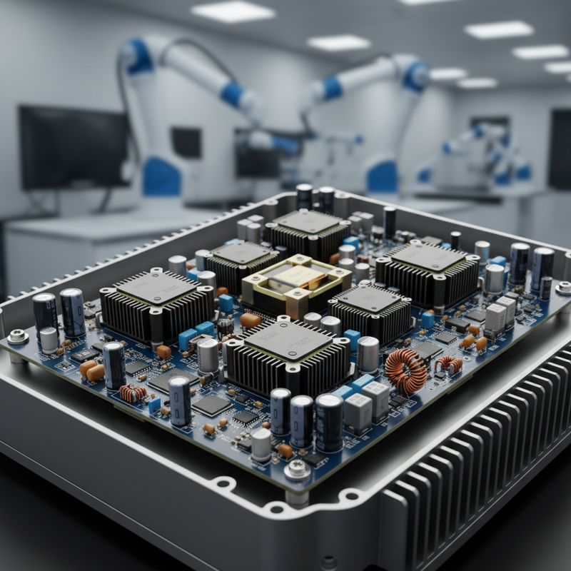
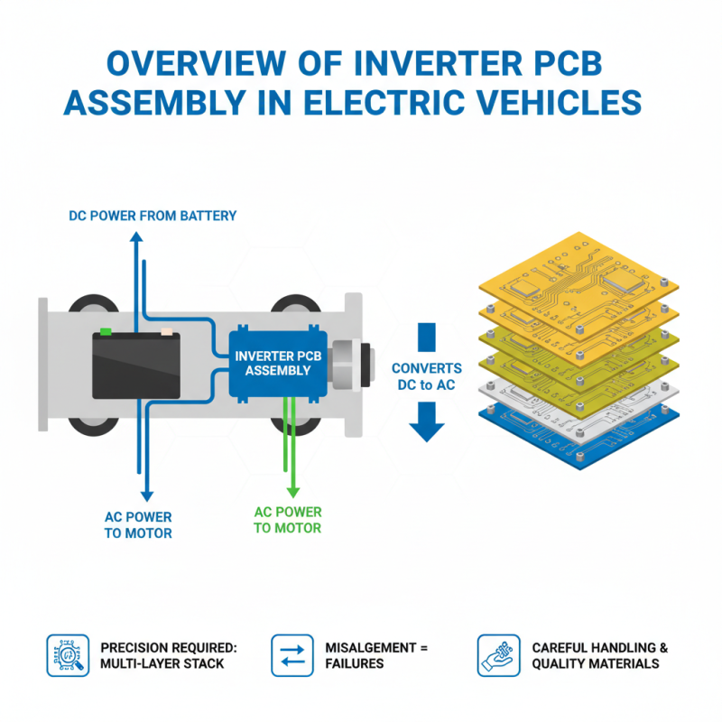
In electric vehicles, inverter PCB assembly plays a crucial role. It converts DC power from batteries into AC power for electric motors. This process is intricate and requires precision. The assembly involves many layers of printed circuit boards, where each layer must be perfectly aligned. Any misalignment can lead to failures. Therefore, careful handling and high-quality materials are essential.
Moreover, the choice of techniques impacts performance. Quick Turn Pcb Assembly can speed up production. However, speed should not compromise quality. Every component needs thorough inspection. It’s easy to overlook small defects, but they can cause significant issues later. Regular testing and validation are vital in this phase. In many cases, engineers discover flaws post-assembly, which emphasizes the need for a meticulous approach.
Lastly, thermal management is another challenge. Inverters generate heat, requiring effective design solutions. Poor heat dissipation can result in reduced efficiency. It’s a balancing act between space, weight, and functionality. Every design decision should be revisited for optimization. Ultimately, the goal is to refine the inverter PCB assembly process to enhance reliability and performance in electric vehicles.
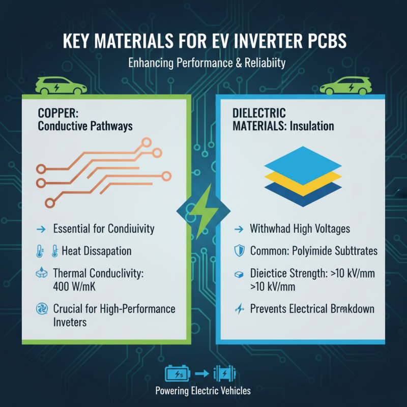
Inverter PCB assembly for electric vehicles (EVs) relies on specific key materials. These materials directly impact performance and reliability. Copper is essential for conductive pathways. With a thermal conductivity of 400 W/mK, copper efficiently dissipates heat, crucial for high-performance inverters. The dielectric materials used must withstand high voltages. Polyimide substrates are common, offering dielectric strength over 10 kV/mm.
Adhesives and epoxies also play a vital role. They bond components securely, ensuring durability under stress. However, their curing processes can be unpredictable, leading to potential weaknesses. Industry reports indicate a 15% failure rate in inverter assemblies due to poor adhesion. Hence, careful selection and testing of these adhesives are necessary.
The choice of Stencil For Pcb Assembly impacts the precision of component placement. A well-designed stencil ensures optimal solder paste application. However, improper stencil thickness can lead to defects. According to recent studies, nearly 20% of assembly issues stem from stencil-related errors. Using an appropriate stencil design is crucial to achieving high-quality outputs in EV inverters.
Designing inverter PCBs for electric vehicles (EVs) requires careful consideration of various techniques. One key aspect involves optimizing the layout. The placement of components can significantly impact performance. A compact design reduces the path length for signals, which minimizes noise and enhances efficiency. Select materials that withstand high thermal and electrical demands.
Thermal management is another crucial factor. Inverters produce heat during operation. Employing heat sinks and thermal vias helps dissipate heat effectively. This not only improves reliability but also prolongs the lifespan of components. Testing under real-world conditions can reveal unexpected thermal issues. Reassessing designs based on test results is essential.
Finally, consider component integration. Using fewer, multifunctional components can simplify the design. However, ensure that this approach does not compromise reliability. Regular feedback from prototyping can uncover flaws in the layout. The goal is to create a robust inverter while minimizing complexity in the Main Pcb Assembly. Balancing performance and manufacturability is challenging but vital for success.
Inverter PCB manufacturing is crucial for electric vehicles (EVs). A well-designed PCB can significantly enhance performance and efficiency. Recent studies show that up to 75% of EV performance relies on inverter efficiency. As such, understanding manufacturing processes is vital.
One common technique is using multilayer PCBs. They help save space and improve thermal management. According to industry data, multilayer PCBs can reduce thermal resistance by 30%. This is important because heat can affect the inverter's functionality. However, the complexity of multilayer designs brings challenges. Issues like signal integrity can arise, requiring precise design and testing.
Another technique is surface mount technology (SMT). SMT allows for smaller components, which is essential for compact inverter designs. Reports indicate that SMT can increase production efficiency by 50%. Yet, this process requires advanced machines and skilled operators. Misalignment during assembly can lead to costly recalls. Continuous improvement in techniques and processes is necessary to avoid such pitfalls and enhance the overall quality of inverter PCBs for EVs.
Inverter PCB assembly for electric vehicles (EVs) requires rigorous testing and quality control. This process involves detailed inspections to ensure reliability. According to a recent industry report, over 70% of failures in EV inverters can be traced back to PCB defects. Such data highlights the importance of a thorough quality control protocol.
Various testing techniques are employed. Visual inspections are essential. Automated optical inspection (AOI) can detect defects early. This method scans PCBs at high speeds, identifying soldering issues and component misalignments. However, it is not foolproof. Some issues escape visual checks. As reported by tech experts, companies often find that 15% of defects remain undetected until field use.
Functional testing is another crucial method. This ensures each inverter operates within specifications. In a study, it was found that approximately 20% of inverters failed during these tests. Engineers must continually refine their techniques. They need to adapt to evolving technologies. Continuous improvement is vital for maintaining quality in this high-stakes field.
Inverter PCB assembly for electric vehicles (EVs) presents unique challenges. One notable issue is managing heat dissipation. High temperatures can damage components. Proper thermal management techniques are essential for maintaining performance.
Old methods may not suffice. Re-evaluating assembly techniques can lead to better results. Utilizing Surface Mount Pcb Assembly enhances space efficiency. This also improves airflow around vital components. Still, ensure adequate testing processes are in place. Without thorough checks, potential failures may go unnoticed.
Tips: Prioritize reliable soldering techniques. Poor solder joints can lead to failures. Also, consider how your design affects assembly. Complex layouts might complicate the process. Reflect on current practices. Adjustments may be necessary for better outcomes. Collaboration with engineers can yield valuable insights.
The future of inverter PCB technology for electric vehicles (EVs) is rapidly evolving. Industry reports estimate that the demand for EVs will exceed 30 million units by 2030. This surge drives innovation in PCB design and assembly techniques, as they are critical for enhancing efficiency and performance. Sophisticated cooling solutions are on the rise, improving thermal management in inverters, which is vital for durability.
Tips to consider involve PCB material selection. High thermal conductivity materials can improve performance significantly. Always assess the operating environment, as extreme conditions can affect PCB longevity.
Moreover, modular designs are trending. They allow for easier upgrades and repairs. However, achieving modularity without compromising space and weight can be challenging. Manufacturers need to rethink their assembly processes. Continuous testing and prototyping can identify flaws early.
Using advanced simulation tools can streamline this process. They provide insights but can also create a false sense of security. Not all anomalies can be captured in simulations. Real-world testing is still essential, despite technological advancements. It’s crucial to keep refining methods for better reliability and efficiency.
| Technique | Description | Future Trends |
|---|---|---|
| Surface Mount Technology (SMT) | A technique that allows components to be mounted directly onto the surface of printed circuit boards. | Increasing use of smaller components and improved automation in assembly. |
| Through-Hole Technology | Components are inserted into holes drilled in the circuit board and soldered from the opposite side. | Adoption in high-reliability applications where durability is crucial. |
| Automated Optical Inspection (AOI) | Using cameras to inspect PCBs for defects during production. | Integration with AI for enhanced defect detection capabilities. |
| Thermal Management | Techniques to control heat generation and dissipation in PCB assemblies. | Increased focus on advanced materials for better heat resistance. |
| Flexible PCB Technology | PCBs that can bend and flex, allowing for innovative designs in space-constrained applications. | Growing adoption in complex EV systems requiring adaptable layouts. |
The field of electronics is rapidly evolving, and advancements in PCB technology are at the forefront of this development. A notable innovation is the creation of 6-layer high-frequency hybrid circuits that utilize cutting-edge materials such as Rogers RO4350B and S1000. These materials are specifically designed for high-frequency applications, offering low loss and exceptional stability, which are crucial parameters for reliable signal processing in modern electronic devices.
One of the standout features of these hybrid PCBs is their metal edging, which not only enhances mechanical strength but also provides a robust shield against electromagnetic interference. This design consideration ensures that signals remain stable and clear, even in complex operational environments. Additionally, employing advanced manufacturing techniques leads to impressive precision—boasting a minimum via size of 0.25mm and a line width/space of 5/5mil. Such specifications enable high-density wiring, making it possible to integrate more components efficiently on a compact circuit board.
The combination of precise impedance control and adequate copper thickness results in efficient signal transmission and power stability, essential for applications in fast-paced domains like 5G communication, aerospace, and automotive electronics. This mature manufacturing process, characterized by one-time pressing and drilling, guarantees that these hybrid circuits are not only reliable but also contribute considerably to the overall performance of the final electronic products.
: Copper is critical for conductive pathways and heat dissipation. Polyimide substrates are used for high voltage applications.
Adhesives ensure component durability. However, curing processes can be unpredictable, risking assembly weaknesses.
There is a 15% failure rate due to poor adhesion, indicating the need for careful adhesive selection and testing.
Proper stencil design improves solder paste application. Poor stencil thickness can lead to significant defects.
About 20% of assembly issues stem from problems related to stencil design or application.
Increased demand for EVs is driving innovations. Sophisticated cooling solutions are becoming essential for thermal management.
High thermal conductivity materials improve performance. Assess the operational environment for longevity concerns.
Balancing modularity with space and weight is difficult. Rethinking assembly processes is necessary to overcome this challenge.
They provide valuable insights but might give a false sense of security. Real-world testing remains crucial.
It helps identify flaws early. Continuous refinement of methods is needed for better efficiency and reliability.
Inverter PCB Assembly for EVs plays a crucial role in the efficiency and performance of electric vehicles. This process involves selecting key materials that ensure durability and optimal conductivity, which are essential for handling high power and heat dissipation. Employing advanced design techniques allows engineers to enhance the functionality of inverter PCBs while ensuring they meet the stringent requirements of modern EVs.
Moreover, the manufacturing processes adopted for Inverter PCB Assembly are critical, encompassing precision fabrication and assembly methods that support high volume production. Testing and quality control measures are vital to guarantee reliability and safety. Despite facing common challenges, such as thermal management and component integration, ongoing advancements in inverter technology promise to drive innovation and efficiency in the EV sector. The future of Inverter PCB Assembly for EVs looks promising with anticipated improvements in materials and techniques.