In today’s fast-changing world of electronics, you really can’t overlook how important HDI PCB manufacturing is. As gadgets get smaller, more powerful, and way more efficient, manufacturers gotta stay ahead of the curve with advanced techniques to keep up with tech’s rising demands. Shenzhen Rich Full Joy Electronics Co., Ltd., a national high-tech and innovative company, is right there at the forefront of this shift. They blend expertise and a focused approach to bring some seriously cutting-edge solutions to the table. Recognized as a key hub for startups and new businesses in China, their commitment to top-quality HDI PCB production means they’re all set to support the next wave of electronic devices. In this blog, I’ll dive into why HDI PCB manufacturing is such a big deal and share some of the best strategies to make it even more efficient — because honestly, it’s shaping what the future of electronics looks like.
The Significance of HDI PCB Manufacturing in Contemporary Electronic Devices
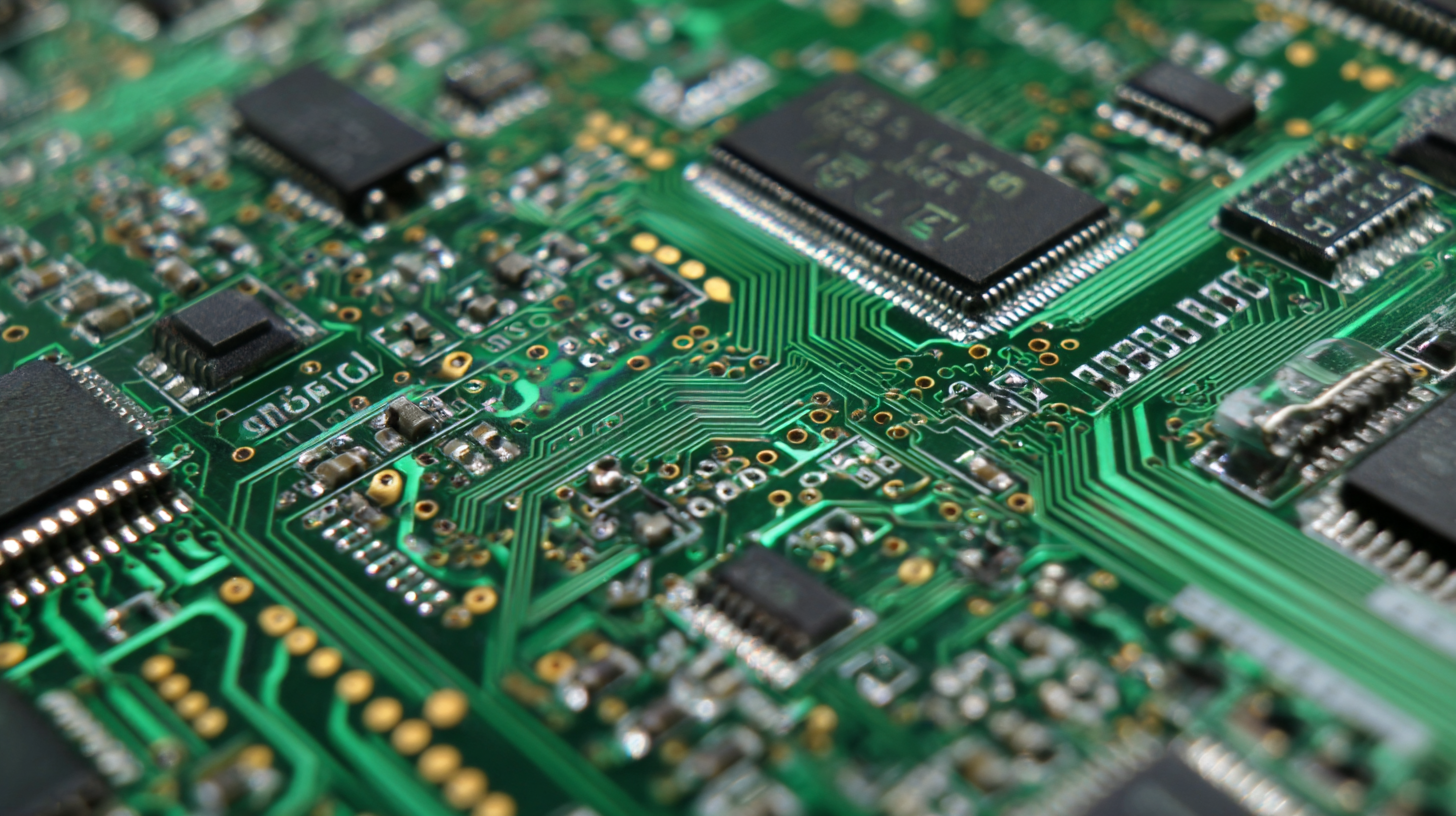
You know, when it comes to today’s tech gadgets, HDI PCB manufacturing really plays a huge role — it’s pretty much impossible to overstate its importance. As the electronics world shifts towards smaller, sleeker devices, these high-density interconnect (or HDI) tech becomes more and more essential. They help create those tiny, yet powerful gadgets packed with features we all love. By around 2025, we’re expecting the market for niche materials like electronic-grade oxidized copper to grow a lot, which just shows how crucial it is to use high-quality, pure materials when making PCBs.
And honestly, it’s not just about making things smaller anymore. The rise of 5G? That’s throwing a whole new set of challenges into the mix. Unlike older tech, 5G needs faster speeds, higher data capacity, and less lag — all of which demand super innovative design and manufacturing tricks. To keep up with these intense requirements, manufacturers really need to adopt the latest techniques, especially since high-frequency signals add extra layers of complexity.
A couple of tips for engineers working on HDI PCBs: first, layout is everything — plan carefully to keep signals clear and avoid interference. Also, don’t forget about heat — managing it well helps keep everything running smoothly and reliably. And of course, staying updated with the latest manufacturing capabilities is key, especially with the industry evolving so fast. It’s all about staying a step ahead to meet these high-tech demands.
Key Advantages of HDI PCBs Over Traditional PCB Types
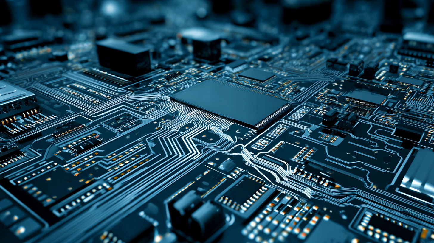
High-Density Interconnect (HDI) PCBs are really changing the game in modern electronics. They've got some pretty impressive perks compared to the old-school types. For starters, they can pack way more components into a tiny space — all thanks to thinner lines and smaller gaps, plus some cool manufacturing tricks like microvias and buried vias. This means you get a much higher circuit density without making the board bigger. As gadgets keep getting smaller and sleeker, HDI PCBs are becoming absolutely essential, especially in compact stuff like smartphones, tablets, and wearables.
But it's not just about fitting more in a small package. HDI PCBs actually boost overall performance and reliability too. Because signals travel shorter distances and there's less electromagnetic interference, they improve signal quality and speed — perfect for high-frequency tech. Plus, their multi-layer setup helps distribute power and ground more efficiently, cutting down on power loss and heat issues. All of this not only amps up the device’s performance but also helps it last longer. So, both manufacturers and users end up with more durable, efficient gadgets in the long run.
What is the Importance of Hdi Pcb Manufacturing Process in Modern Electronics - Key Advantages of HDI PCBs Over Traditional PCB Types
| Advantage |
HDI PCB |
Traditional PCB |
| Density |
Higher density with smaller vias |
Lower density with larger vias |
| Size |
Compact and lightweight |
Bulkier, often larger footprint |
| Signal Integrity |
Improved signal integrity and reduced path length |
Potentially lower signal integrity |
| Manufacturing Cost |
Higher initial cost, but often more cost-effective in the long run |
Lower initial cost, but less efficient |
| Thermal Management |
Better thermal performance |
Less efficient thermal management |
| Application Range |
Suitable for high-speed and high-performance applications |
Suitable for general applications |
Comparative Analysis of Production Techniques for HDI PCBs
You know, High-Density Interconnect (HDI) PCBs have become pretty much essential in today's tech world. That's mainly because they're so good at handling miniaturized and complex designs—things we've come to expect from modern gadgets. When you look at how these boards are made, techniques like laser drilling, microvia technology, and sequential lamination really stand out. According to a report from Research and Markets, the HDI PCB market is expected to hit around $23.2 billion by 2025. That’s mainly thanks to smartphones and IoT devices becoming more widespread—that's what makes efficient manufacturing methods so important.
Take laser drilling, for example. It lets manufacturers create tiny vias with a level of precision that traditional methods just can’t match. This not only helps improve signal quality but also cuts down on power consumption—pretty crucial for high-performance gear. Then there’s the sequential lamination process, which gives designers more freedom with how they stack layers, opening doors for more sophisticated designs—think telecom and automotive industries. Interestingly, studies suggest that HDI boards can cut overall weight by about 25%, which is a big deal for aerospace and portable electronics.
Of course, the choice of manufacturing technique doesn’t just influence how well the PCB performs but also how much it costs to produce. That’s why there’s always a push for innovation in HDI PCB manufacturing—things are moving so fast, it’s hard to keep up!
Evaluating HDI PCB Cost-Effectiveness in Modern Electronics
As people keep pushing for smaller, faster, and more efficient gadgets, High-Density Interconnect (HDI) PCBs have really become a key player in today’s electronics scene. I mean, according to Fortune Business Insights, the global HDI PCB market is expected to hit around $31 billion by 2026, growing at nearly 9% annually from 2019 through 2026. That’s mainly because everyone’s on the lookout for compact devices—whether it’s your smartphone, car tech, or other gadgets—so the need keeps climbing.
Now, if you're wondering about whether HDI PCBs are worth the cost, it’s a bit of a balancing act. Sure, they can be pricier to manufacture upfront compared to traditional boards, but honestly, the long-term perks really add up. These PCBs allow for tighter routing and take up less space, which not only cuts down on the amount of material used but also helps make the final product smaller and sleeker. Plus, studies show that switching to HDI tech can slash assembly costs by up to 30% and even save about 20% in power consumption. All in all, investing in HDI isn’t just about performance—it's a smart move for manufacturers who want to stay ahead in this super competitive market.
The Importance of HDI PCB Manufacturing Process in Modern Electronics
This bar chart illustrates key evaluation metrics for the HDI PCB manufacturing process in modern electronics. The data reflects cost, performance, complexity, production time, and yield rate, showcasing the effectiveness and importance of HDI PCBs in contemporary electronic designs.
Impact of HDI Technology on Miniaturization and Performance
High-Density Interconnect (HDI) printed circuit boards—yeah, the tiny, intricate boards—have really shaken things up in the world of electronics. They’ve made it possible to pack more power into much smaller devices, which is pretty much what everyone’s after these days. According to some report by Market Research Future, the HDI PCB market’s expected to grow at around 10.5% annually from 2021 to 2027. Basically, that just shows how crucial HDI tech has become for meeting the fast-changing needs of today’s gadgets and tech applications.
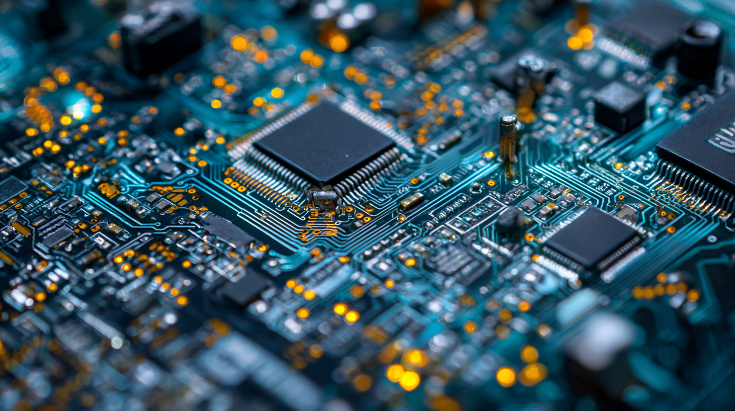
One of the biggest wins with HDI technology has got to be the miniaturization of electronic devices. By using finer traces and smaller vias, HDI PCBs can cram more components onto a single board than the older, bulkier types. An IEEE study mentions that you can 缩小 your PCB size by up to half AND still keep or even boost electrical performance. This kind of shrinkage means manufacturers can create sleeker, more elegant gadgets without skimping on capabilities. It’s no wonder industries like consumer electronics, telecom, and automotive are totally into HDI boards.
And let’s not forget the performance side of things—HDI definitely delivers there, too. With improved routing options and less signal loss, these boards offer way better electrical performance. A 2023 report from IPC even states that signal integrity can improve by up to 30%, which helps devices process data faster and use less power. That’s a huge deal, especially for high-speed stuff like 5G and next-gen computers. So, in a nutshell, HDI boards are not just about making things smaller—they're about making them smarter and more efficient too.
Future Trends in HDI PCB Manufacturing and Their Implications
Looking ahead, the future of High-Density Interconnect (HDI) PCB manufacturing is super exciting, with some pretty remarkable advancements on the horizon. As technology keeps moving forward, there's a growing push to make electronic devices smaller, lighter, and way more efficient — and that’s really driving innovation in how we design and produce PCBs. You know, things like 5G, the Internet of Things, and AI are totally transforming the way HDI PCBs are developed, pushing the limits of traditional manufacturing methods in ways we never really saw before.
At the forefront of all this is Shenzhen Rich Full Joy Electronics Co., Ltd., a truly innovative high-tech company. They’ve got some serious expertise in HDI tech and use cutting-edge manufacturing techniques. This puts them in a great spot to handle the increasing demand for complex electronic setups. They’re not just riding the wave—they’re actively shaping the future with a focus on R&D, so they don’t just follow industry trends—they help set them. Their goal? To support the next wave of smart gadgets and tech, pushing forward in a world that changes faster than ever, but still staying true to quality and innovation every step of the way.
Exploring Market Trends: The Growth and Innovation of Flexible Printed Circuits and Rigid-Flex PCBs in 2023
The growth of the flexible printed circuit board (FPCB) market in 2023 has been driven by the increasing demand for advanced technology in various industries. Specifically, rigid-flex PCBs—multi-layer flex circuits that integrate the strengths of rigid and flexible designs—are experiencing significant innovation and expansion. According to a report by MarketsandMarkets, the global market for rigid-flex PCBs is projected to reach $3.9 billion by 2026, growing at a CAGR of 10.5% from 2021. This growth is largely attributed to their application in high-performance sectors such as medical devices, consumer electronics, and automotive systems.
One of the key advantages of rigid-flex PCBs is their unmatched flexibility, which allows for high-density component placement. This unique design reduces the need for connectors and simplifies assembly processes, ultimately leading to improved reliability and performance in complex electronic systems. Industry experts note that the automotive sector, in particular, is leveraging these technologies to enhance electrical performance and reduce weight. Companies are increasingly adopting rigid-flex solutions to support the rising demand for electric vehicles and advanced driver-assistance systems (ADAS), positioning themselves to remain competitive in a rapidly evolving marketplace.
Moreover, the superior signal integrity offered by rigid-flex PCBs is critical in applications where precision and reliability are paramount. In the fast-paced consumer electronics market, brands are investing in these circuits to innovate products that require smaller form factors without compromising on performance. Research from IDTechEx highlights that the consumer electronics segment is expected to be a major driver of demand, leading to advancements in design and manufacturing technologies that further enhance the capabilities of flexible printed circuits.
FAQS
: HDI PCB manufacturing is essential for meeting the demands of miniaturization and 5G technology, allowing for smaller, more powerful devices that comply with consumer needs.
HDI PCBs can accommodate more components in a smaller area, utilize finer lines and microvias, and provide enhanced performance and reliability compared to traditional PCBs.
High-purity materials, particularly electronic-grade oxidized copper, are crucial for improving the quality and effectiveness of HDI PCB manufacturing.
HDI PCBs offer shorter signal pathways and reduced electromagnetic interference, which enhances signal integrity and speed, making them ideal for high-frequency applications.
Key techniques include laser drilling, which creates precise microvias, and sequential lamination, which allows for flexible layer stacking and advanced designs.
The production technique affects both the performance and cost-efficiency of HDI PCBs, highlighting the importance of innovation in manufacturing methods.
The HDI PCB market is anticipated to reach $23.2 billion by 2025, driven by the rising adoption of smartphones and IoT devices.
Proper heat dissipation is crucial to maintain reliability and performance, particularly in compact devices that generate higher heat levels due to their advanced functionalities.
Microvias are small vias created through advanced drilling techniques that allow for increased circuit density, facilitating more components in a limited space, which is essential for modern electronic devices.
The enhanced performance and reliability of HDI technology can extend the lifecycle of devices, offering greater value to both manufacturers and consumers over time.
Conclusion
HDI PCB manufacturing is a pretty vital part of today’s electronics scene. It’s a key player when it comes to building those super-advanced devices we see everywhere. Basically, by using high-density interconnect tech, HDI PCBs give us a lot of benefits compared to the old-school PCB types — like better performance, smarter miniaturization, and taking up less space. In this blog, I want to unpack some of the main perks of HDI PCBs, compare how they’re made, and look at whether they’re worth your money these days.
By the way, Shenzhen Rich Full Joy Electronics Co., Ltd., is a big name in the industry. They’re really pushing the boundaries with these innovations and helping shape where electronics are headed. The way HDI tech boosts miniaturization and overall performance is pretty exciting and definitely points to a future where everything gets smaller and more powerful. If you’re curious about what’s next for HDI PCB manufacturing, I’ll be diving into some of the latest trends and what they might mean for the market — so stay tuned!