











High-Frequency PCB Surface Finishes: Which One Delivers the Best Solderability and Signal Integrity?
In the world of high-frequency PCB manufacturing, surface finishing is a critical process that directly influences solderability, signal integrity, and overall reliability. As electronic devices evolve toward miniaturization and higher performance, the surface finish must not only protect the copper surface but also ensure high-frequency signal transmission and robust solder joints.
This article explores the pros and cons of common high-frequency PCB surface finishes, identifies potential defect mechanisms, and highlights best practices for quality control—helping engineers make informed, performance-driven decisions.
Common Surface Finishing Technologies for High-Frequency PCBs
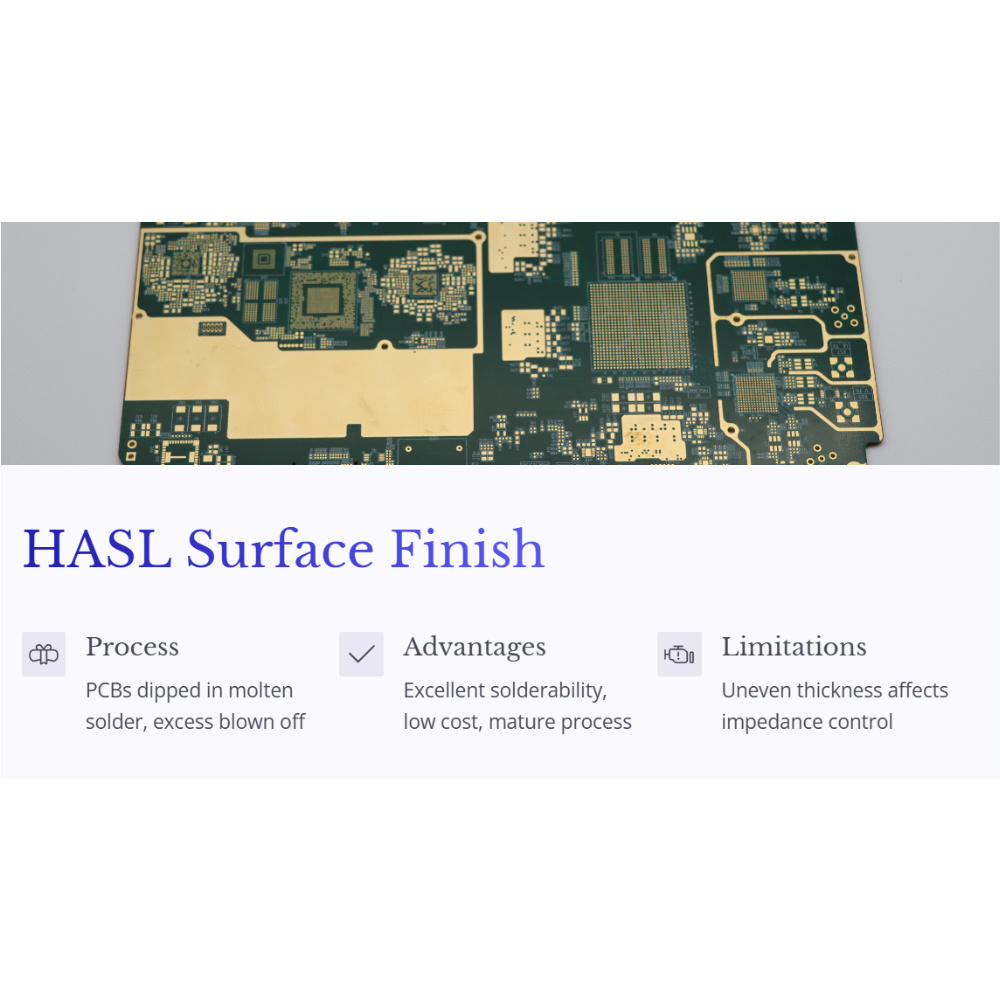
1. HASL (Hot Air Solder Leveling)1. HASL
Process:
PCBs are dipped in molten solder (Sn-Pb or lead-free), then excess solder is blown off using high-pressure hot air, leaving a uniform solder coating.
Advantages:
● Excellent solderability
● Compatible with wave and reflow soldering
● Low cost and mature process
Limitations in RF Applications:
Due to uneven solder thickness, HASL may introduce impedance variation, impacting high-frequency signal integrity—especially in fine-line designs where precise impedance control is critical.
2. ENIG (Electroless Nickel Immersion Gold)
Process:
A thin nickel layer is chemically deposited to act as a barrier, followed by an immersion gold layer that enhances solderability and contact performance.
Advantages:
● Uniform, flat surface
● Excellent corrosion and oxidation resistance
● Stable electrical performance in high-frequency environments
Challenges:
ENIG has a higher cost, and poor control of the nickel layer can lead to "black pad" defects, severely impacting solder joint quality and reliability.
3. OSP (Organic Solderability Preservative)
Process:
Forms a thin, organic coating over the copper surface to prevent oxidation. The layer decomposes during soldering, exposing clean copper for bonding.
Advantages:
● Cost-effective and simple
● Ideal for fine-pitch components and high-frequency circuits (minimal impact on impedance)
● Excellent flatness
Drawbacks:
● Short shelf life
● Poor durability in harsh environments
● Surface can be easily contaminated, compromising solderability
4. Immersion Silver
Process:
A thin layer of silver is deposited via a chemical displacement reaction, offering a smooth, conductive finish.
Advantages:
● High conductivity and good solderability
● Minimal signal loss for RF applications
● Moderate cost
Drawbacks:
● Prone to sulfidation and discoloration in sulfur-rich environments
● Risk of silver migration under improper soldering conditions, affecting long-term reliability
Defect Mechanisms and Reliability Impact
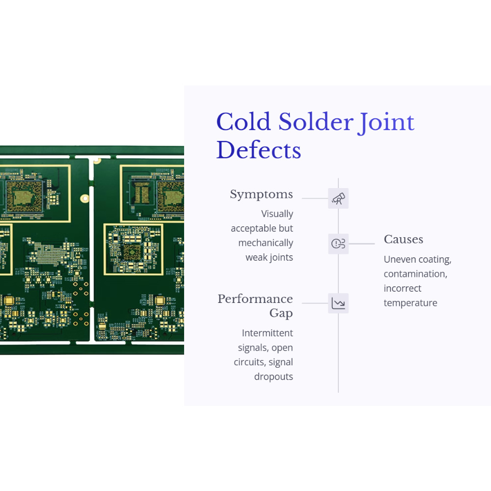
1. Cold Solder Joints
Symptoms:
Visually acceptable joints that are actually mechanically weak—prone to failure under vibration or thermal stress. Microscopy reveals microgaps and poor intermetallic bonding.
Causes:
● Uneven coating thickness (especially in HASL)
● Surface contamination (e.g., OSP absorbing dust or oils)
● Incorrect soldering temperature or time
Performance Gap:
Well-treated PCBs exhibit shiny, robust solder joints with strong metallurgical bonds. Cold joints result in intermittent signals, open circuits, and signal dropouts in RF systems.
2. Corrosion and Oxidation
Symptoms:
Visible discoloration—greenish copper oxide or black spots. OSP can degrade in humid environments, and silver can darken due to sulfide exposure.
Causes:
● Insufficient protective layer (thin OSP or poor silver coating)
● Harsh storage conditions (high humidity, corrosive gases)
● Residual chemicals left after manufacturing
Performance Gap:
Properly protected PCBs retain solderability and electrical integrity for extended periods. Oxidized surfaces hinder wetting, reduce joint reliability, and cause increased surface resistance, degrading high-frequency performance.
3. Plating Layer Defects
Symptoms:
In ENIG, possible defects include nickel voids and gold layer non-uniformity. In Immersion Silver, rough surfaces or pinholes may form. These are detectable via X-ray or microscopy.
Causes:
● Unstable bath chemistry (e.g., incorrect pH, metal ion concentrations)
● Contaminated plating solutions
● Inconsistent time and temperature control
Performance Gap:
High-quality finishes ensure signal consistency and reliable soldering. Plating defects can lead to signal reflection, EMI, or open circuits, especially in sensitive RF applications.

Rich Full Joy’s Surface Finishing Expertise for High-Frequency PCBs
At Rich Full Joy, we understand that surface finish is not a one-size-fits-all solution—especially in high-frequency PCB manufacturing. With years of RF experience and a portfolio of advanced surface treatment equipment, we offer:
● Process selection tailored to your application
● Precision control of plating thickness and uniformity
● Cleanroom-level contamination control
● Rigorous quality assurance using AOI, X-ray, and cross-sectional analysis
Our team ensures every PCB meets your solderability, reliability, and signal integrity needs—so your products succeed, even in the most demanding environments.









