











High Layer Count PCB (>12L) Lamination Registration: How Cumulative Tolerance Eats Your High-Density Routing Window
Designing a 16-layer, 20-layer, or even 24-layer PCB with high-density interconnect features feels like a precision engineering triumph — until the boards come back from fabrication and microvias are breaking out of their capture pads. The root cause is rarely a single gross error. More often, it is the quiet, relentless accumulation of small deviations across every layer and every process step. In high layer count PCB fabrication, cumulative tolerance is not a line item on a datasheet; it is a silent predator that systematically erodes your routing window, layer by layer. For any PCB manufacturer serving applications that push layer counts beyond twelve, mastering this accumulation is the difference between first-pass yield and a protracted, costly debug cycle.
At RICHFULLJOY, where our PCB fabrication and PCBA service teams routinely build complex multilayer boards for networking, aerospace, and medical imaging, we see the same pattern repeat: a design that passes DRC with comfortable margins fails in practice because the registration budget was derived from single-layer assumptions. Once the board stackup crosses the 12-layer threshold, the physics of material movement, lamination dynamics, and drill wander interact in ways that linear tolerance stackups cannot capture. Understanding this interaction — and designing for it — is essential for anyone pushing the boundaries of HDI routing density.
Why 12 Layers Is the Registration Inflection Point
Most PCB designers are comfortable with 4- to 8-layer stackups. The core count is low, the lamination cycles are few, and the total material movement across the stack remains manageable. At these layer counts, a well-controlled fabrication process can hold layer-to-layer registration to within ±2 mil or better, and the annular ring requirements for buried and blind vias can be met with standard design rules.
Beyond twelve layers, three compounding factors emerge:
Multiple Lamination Cycles: A 16-layer board is typically built as two 8-layer sub-cores laminated together, or as sequential laminations. Each lamination cycle introduces its own material movement — core expansion, resin flow, and mechanical misalignment of tooling holes. These movements are not independent; they stack statistically, and the probability of cancellation is low.
Asymmetric Copper Distribution: High layer count PCBs for high-speed digital or RF applications often feature asymmetric copper densities across the stack. Power planes on one side and sparse routing on the other create thermal expansion mismatches during lamination cool-down, warping the sub-cores and shifting features relative to the global drill coordinate system.
Thinner Dielectrics, Higher Stakes: To keep overall thickness manageable, designers use thinner prepregs and cores. Thinner dielectrics mean less mechanical stiffness, making the sub-assembly more susceptible to handling distortion during layup. At the same time, high-density routing demands tighter via-land tolerances, so the error budget that was generous at 8 layers collapses just when you need it most.
This inflection point is where many high layer count PCB fabrication projects encounter reality. The registration performance that a fabricator guarantees on their process capability datasheet was typically characterized on test vehicles with balanced, moderate layer counts. Extrapolating those numbers to a 20-layer board with sequential lamination and buried microvias is, at best, an informed guess — unless the fabricator has production data from similar builds.
The Anatomy of Cumulative Registration Error
To understand how tolerance accumulates, we need to decompose registration error into its constituent sources. Each contributes a small displacement vector; the net misalignment at any given layer is the vector sum of these contributions from every preceding process step.
Core Dimensional Instability: The Baseline Drift
Every laminate core expands and contracts with temperature and moisture content. When a core is imaged with a laser direct imaging (LDI) system, it is registered to the tooling holes drilled at room temperature. During lamination, the core heats to 180–200 °C, expands, becomes compliant as the resin melts, and then solidifies under pressure. When the finished board returns to room temperature, the core dimensions have shifted relative to the original imaging coordinate system. For a standard FR-4 core 18 × 24 inches, this movement can easily reach ±3–4 mils in the warp and fill directions — and it is almost never isotropic. The glass weave style (e.g., 1080, 2116, 7628) dictates different coefficients of thermal expansion along warp and fill, so the displacement is directional and layer-dependent.
In a 16-layer board with four different core types, each core moves differently during its own lamination cycle. Subsequent lamination cycles then move the entire sub-assembly again. The result is that a given inner layer’s features are not where the final drill file expects them to be. This is the starting point of the cumulative tolerance stack.
Layer-to-Layer Alignment During Layup
Before lamination, the individual cores and prepreg sheets are stacked on alignment pins or a layup fixture. The alignment depends on the clearance between the tooling holes and the pins. A 0.5 mil clearance per hole might sound negligible, but across multiple cores and prepreg layers — each with its own tooling holes drilled at a different time, potentially on a different drill machine — the angular misalignment can introduce a tangential displacement that grows with distance from the alignment pins. On a large panel, a 0.2° rotation from pin clearance translates to a 10-mil displacement at the far corner.
In a sequential lamination process, where already-laminated sub-cores are re-drilled and re-stacked, the accumulation of pin-clearance rotation errors becomes geometric, not linear. Each lamination step rotates the coordinate system by a small angle, and the next sub-core is aligned to the now-rotated pins. After three sequential laminations, the net rotation can be 0.5° or more, pushing edge features completely out of tolerance — even though each individual step was within spec.
Drilling Registration: The Last Displacement
After lamination, the finished board is drilled for through-holes and back-drilled vias. The drill machine uses the same tooling holes for registration — but those holes have now undergone the dimensional drift of the entire stackup. If the board has shrunk asymmetrically, the drill program’s linear scaling correction can only partially compensate. The residual error — typically a few mils — adds on top of all the inner-layer misregistrations.
For a buried via that must land on an inner-layer pad originally imaged three lamination cycles earlier, the total misregistration is the sum of: core movement during first imaging, first lamination drift, second lamination rotation, third lamination drift, and final drill offset. At each step, the error can be 2–3 mils. By the time the drill breaks through, the via can miss its target by 6–8 mils or more. This is the “cumulative tolerance” that consumes the routing window.
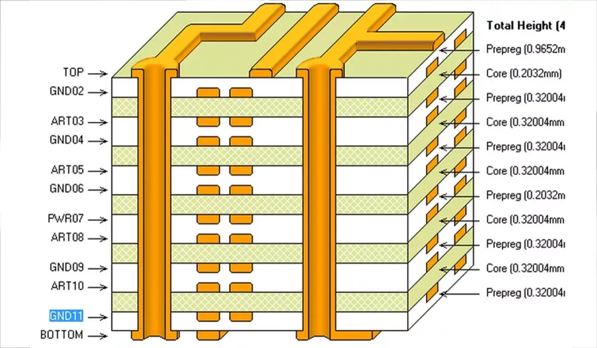
How Cumulative Tolerance Devours Your Routing Window
Microvia Annular Ring Collapse
The most visible victim of cumulative registration error is the microvia capture pad. In a typical HDI design with 0.1 mm (4 mil) laser vias, the recommended capture pad diameter is 0.3 mm (12 mil) to ensure a 4-mil annular ring around the via hole. The IPC-6012 Class 3 requirement for annular ring is 2 mils minimum. On paper, a 12-mil pad with a 4-mil via and 6-mil finished hole size provides a 3-mil annular ring — sufficient margin.
But this calculation assumes perfect alignment between the laser via and the inner-layer pad. In a >12-layer board with sequential lamination, the inner-layer pad may have moved 4 mils relative to the laser drill coordinate. The resulting annular ring is not 3 mils; it is -1 mil (breakout) or a sliver that violates Class 3 requirements. The designer who allocated 2 mils of annular ring margin based on a single-lamination assumption now faces a board that cannot pass acceptance testing — and the failure was not in the fabricator’s capability but in the registration budget the design assumed.
High-Density Routing Clearance Erosion
Beyond via pads, the same accumulation eats into trace-to-trace and trace-to-pad clearances. A differential pair routed with 3.5-mil trace and space on an inner layer depends on that layer’s features staying where the artwork placed them. If the entire layer shifts by 3 mils relative to the adjacent reference plane, the impedance profile of the differential pair changes because the coupling to the plane geometry is altered. Even worse, if the shift is rotational rather than translational, the trace may approach the edge of an anti-pad opening in the plane, creating an impedance discontinuity that no post-layout simulation predicted.
For HDI PCB designs pushing 2-mil lines and spaces, the available routing window between via pads may be only 6–8 mils wide. A 3-mil registration error does not just shrink the window — it can close it entirely, forcing a redesign that sacrifices density or layer count.
Design Strategies That Survive Registration Reality
The most effective way to protect the routing window is not to demand impossibly tight fabrication tolerances, but to design with an honest registration budget informed by the specific stackup and lamination sequence.
Registration Budget Modeling: Worst-Case vs. Statistical
Designers often default to a simple worst-case arithmetic sum: core movement + lamination shift + drill offset = total error. For a >12-layer board with sequential laminations, this sum can exceed 10 mils, making high-density routing seemingly impossible. But the worst-case arithmetic sum is statistically improbable. The various error components — core expansion, pin rotation, drill offset — are not perfectly correlated. A root-sum-square (RSS) statistical model, validated by production data for the specific stackup configuration, can reduce the predicted error to 5–6 mils — still significant, but manageable with proper pad sizing and routing rules.
RICHFULLJOY works with customers during the design phase to provide stackup-specific registration capability data, drawn from historical measurements on similar builds. This data allows the registration budget to be modeled statistically rather than worst-case, freeing up routing real estate while maintaining yield.
Dynamic Annular Ring Rules
A fixed annular ring requirement — say, 5 mils for all microvias — is wasteful on layers near the top of the stack where cumulative error is small, and dangerous on deep layers where error is large. A better approach is a tiered annular ring specification that increases with the number of lamination cycles between imaging and final drill. A via connecting layers 1–2 might only need a 3-mil ring; the same via connecting layers 1–14 might require 6 mils. This keeps the overall design compact while protecting the most vulnerable interconnects.
Rotational Symmetry and Distributed Tooling Holes
To combat rotational alignment errors in sequential lamination, designers can work with their PCB manufacturer to place additional tooling targets near the corners of each sub-core, not just at the traditional four corners. Distributed fiducials allow the fabricator to measure and compensate for intra-panel scaling and rotation at each lamination step, using LDI to dynamically scale the artwork per sub-panel. This approach can reduce net rotation by 50% or more compared to conventional four-slot tooling.
Manufacturing Controls That Preserve the Window
While the designer sets the budget, the PCB fabrication process determines how much of that budget is actually consumed. At the high layer count frontier, process capability is not static — it is actively engineered through three control domains.
Material Preconditioning and Dimensional Stabilization
The most effective way to reduce core movement is to stabilize the laminate before imaging. Baking cores to drive out moisture and relieve internal stresses, then allowing them to equilibrate in a controlled environment, reduces the irreversible shrinkage that occurs during the first lamination cycle. For polyimide or high-Tg FR-4 materials, a controlled thermal excursion that simulates the lamination profile — a “pre-shrink” bake — can remove much of the dimensional change before any copper is patterned. This step adds cost and cycle time, but on a 20-layer board where registration margin is measured in single mils, it is frequently the single highest-leverage process investment.
Lamination Fixture Precision and Press Profiling
The alignment pins and layup plates used in multilayer lamination are consumable tooling that wears with each cycle. At RICHFULLJOY, pin diameter and plate flatness are checked on a cycle-count basis, and fixtures are replaced before wear introduces measurable play. More importantly, the lamination press profile — heat-up rate, pressure application point, and cool-down gradient — is tailored to the specific resin system and stackup geometry. A press profile that cools too quickly freezes in thermal stresses that manifest as warp and subsequent drill misregistration. A profile that applies full pressure too early, before the prepreg has reached minimum viscosity, can shift layers mechanically. These are not standard parameters; they are stackup-specific recipes developed through empirical iteration on actual product panels.
LDI Adaptive Scaling and Layer-Specific Compensation
Laser direct imaging replaces traditional phototools with a programmable laser that can scale the artwork dynamically. Before imaging each inner layer, the LDI system measures the actual positions of fiducials on the core and stretches or compresses the image to match. In a sequential lamination flow, this means each layer’s artwork can be compensated for the core movement that has already occurred, rather than relying on an assumed shrink factor. The result is that the accumulated error at each step is reset, rather than compounded. When combined with post-etch punch systems that re-establish tooling holes based on the imaged pattern, LDI adaptive scaling can hold cumulative registration on 20-layer boards to within 4 mils — a figure that linear shrink compensation alone cannot achieve.
Closing the Loop: From Fabrication to Assembly
The registration story does not end when the bare board passes electrical test. During PCBA service — especially for large BGA packages or press-fit connectors — the same cumulative tolerance that challenged via capture pads now challenges component placement. A BGA with 0.8 mm pitch demands that every pad on the board aligns with its corresponding ball on the package. If the PCB’s global scaling error is 0.03%, that translates to a 3-mil displacement across a 10-inch board — enough to cause head-in-pillow defects on corner balls.
For this reason, RICHFULLJOY’s approach links PCB fabrication data directly to the assembly process. We provide per-panel scaling data so that pick-and-place programs can apply linear compensation if required. This integration between PCB manufacturer and PCBA provider eliminates the finger-pointing that often occurs when high-layer-count boards fail at assembly and the root cause traces back to an uncommunicated registration drift.
The push toward higher layer counts and finer features will not reverse. What must change is the sophistication with which registration tolerance is understood, budgeted, and controlled — from the schematic all the way through the lamination press. A routing window that looks generous in a CAD tool is only as real as the accumulation of every micron of movement across every process step. Working with a PCB fabrication partner who can quantify that accumulation — and who engineers their process to minimize it — is what keeps high-density designs viable when the layer count climbs past twelve.
At RICHFULLJOY, we bring that layer-count-specific process engineering to every high-rise stackup, ensuring that the routing window you draw is the routing window you get.
Frequently Asked Questions (FAQ)
1. What is registration in PCB fabrication, and why does it matter for high layer count boards?
Registration is the positional alignment of features (pads, traces, vias) on different layers relative to each other. In high layer count boards, misregistration can cause microvia breakout, impedance shifts, and clearance violations, directly affecting electrical performance and manufacturability.
2. At what layer count does cumulative tolerance become a significant problem?
Cumulative tolerance effects become pronounced beyond 12 layers, especially when the design uses sequential laminations. Below 8 layers, standard registration budgets are usually adequate; above 12, the interaction of multiple lamination cycles makes error accumulation nonlinear.
3. How does sequential lamination amplify registration error?
Each sequential lamination cycle introduces its own material movement, pin alignment rotation, and drill offset. These errors combine geometrically rather than simply adding, because each cycle references a coordinate system that has already shifted from the original design intent.
4. What is the difference between worst-case and statistical tolerance analysis for PCB registration?
Worst-case analysis sums all error sources arithmetically, often over-predicting misalignment and forcing conservative design rules. Statistical (RSS) analysis accounts for the low probability of all errors peaking in the same direction, providing a more realistic — and still safe — registration budget when based on production data.
5. How can designers protect the routing window in high layer count HDI boards?
Designers can use tiered annular ring rules that increase with lamination depth, model registration budgets statistically, distribute tooling fiducials to combat rotation, and engage their PCB manufacturer early for stackup-specific capability data.
6. What role does laminate material stability play in registration control?
Different laminate materials have different coefficients of thermal expansion (CTE) and moisture absorption. Dimensional changes from these factors during lamination directly cause core movement. Material preconditioning and matching CTEs across the stackup help minimize baseline drift.
7. How does laser direct imaging (LDI) improve registration in multilayer PCBs?
LDI enables per-layer adaptive scaling based on actual fiducial positions on the core, resetting accumulated error at each imaging step. This is significantly more effective than fixed phototool scaling, especially in sequential lamination processes.
8. Can cumulative registration error affect PCB assembly yields?
Yes. Global scaling errors from PCB registration can misalign BGA pads relative to the package, causing solder joint defects. For high-layer-count boards, sharing panel scaling data between fabrication and assembly is critical to maintaining yield.
9. What is the typical registration tolerance a good PCB manufacturer can achieve on a 20-layer board?
With optimized material handling, precision lamination fixturing, and LDI adaptive scaling, experienced manufacturers can hold cumulative registration to within ±4–5 mils on a well-designed 20-layer stackup. The exact capability depends on the specific materials and lamination architecture.
10. How does RICHFULLJOY approach registration control for high layer count PCBs?
RICHFULLJOY combines material preconditioning, stackup-specific lamination profiling, wear-managed tooling, LDI adaptive scaling, and per-panel measurement feedback to minimize cumulative registration error, working with designers from the stackup definition phase to ensure the routing window remains intact through fabrication and assembly.









