Insight into Common HDI Circuit Board Types and Their Applications —— Professional Interpretation by Rich Full Joy
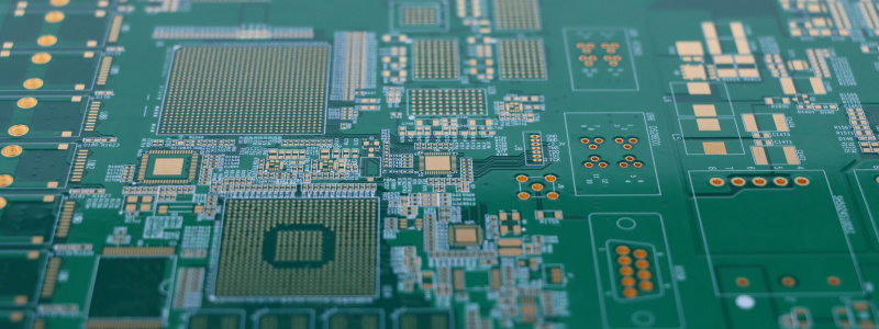
In the current era of the rapid development of electronic products towards miniaturization and high - performance, HDI (High Density Interconnect) circuit boards, with their excellent high - density wiring and complex interconnection structures, have become the core force driving the technological innovation of electronic devices.
Shenzhen Rich Full Joy Electronics Co., Ltd, as a leading enterprise in the electronic circuit field with years of in - depth experience, has always been at the forefront of HDI circuit board technology research and development, manufacturing, and innovative applications.
Next, with our profound professional knowledge, we will take you on an in - depth exploration of common HDI circuit board types, the technical mysteries behind them, their industry application values, as well as the key production process flows and quality control points.
Basic Type Based on the Combination of Rigidity and Flexibility: 1+N+1 Layers
This type of HDI circuit board has a precisely constructed sandwich - like structure in its structural design. The upper and lower layers are durable Rigid PCBs (Rigid Printed Circuit Boards), which serve as the supporting framework of the entire circuit board. They provide a stable physical foundation for the installation of electronic components, ensuring that the circuit board can maintain its structural integrity in complex usage environments and that the electrical connections between electronic components are not affected.
The “N” layers in the middle are Flex PCBs (Flexible Printed Circuit Boards), where the value of “N” can be flexibly adjusted according to the requirements of the actual application scenarios. The Flex PCB layers endow the circuit board with excellent flexibility, enabling special functions such as bending and folding.
In the field of wearable devices, the advantages of this structure are fully demonstrated. For example, in the circuit board of a smart bracelet, the rigid part can stably carry key components such as core chips and sensors, ensuring the stability of data processing and signal collection. The flexible part can skillfully fit the curve of the human wrist, providing a compact and comfortable wearing experience. At the same time, it ensures that during daily activities, the circuit connection is not affected by limb movements, maintaining the normal operation of the device.
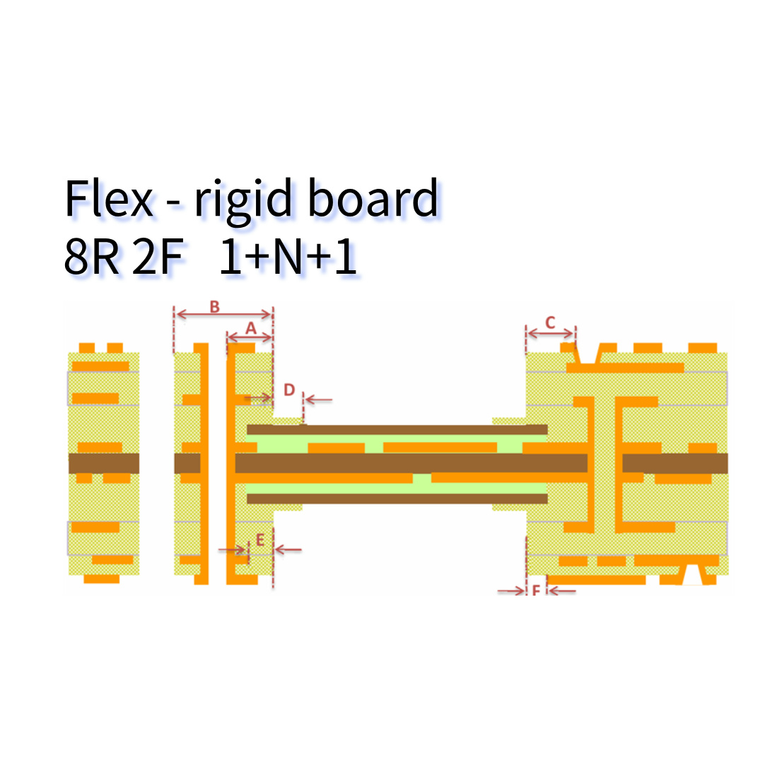
From a technical implementation perspective, in the manufacturing process of the 1+N+1 - layer structure, the connection process between the rigid layer and the flexible layer is of crucial importance. Shenzhen Rich Full Joy Electronics Co., Ltd. adopts advanced lamination technology and precisely controls parameters such as temperature, pressure, and time to ensure seamless connection between the rigid layer and the flexible layer, with stable and reliable electrical performance.
At the same time, in the circuit design of the flexible layer, we use high - precision laser drilling technology to create micro - holes and achieve high - density wiring, meeting the stringent requirements of wearable devices for miniaturization and high performance.
When producing 1+N+1 - layer HDI circuit boards, in the inner - layer circuit manufacturing process, the rigid layer and the flexible layer are respectively lithographed and etched according to their own circuit designs to ensure circuit accuracy.
During the lamination stage, special attention is paid to the selection of prepregs between the rigid layer and the flexible layer and the fine - tuning of lamination parameters to ensure good bonding between layers of different materials.
When drilling and copper - plating, in view of the characteristics of the flexible layer, the laser drilling parameters are optimized to avoid excessive damage to the flexible material, and at the same time, the uniformity and adhesion of the copper - plating layer on the flexible hole wall are ensured.
Key quality - control points (specific to the 1+N+1 - layer structure): Before laminating the rigid layer and the flexible layer, the edges of the rigid layer and the flexible layer are strictly inspected for flatness to prevent poor lamination caused by uneven edges.
After laser drilling of the flexible layer, the quality of the hole wall is inspected under a microscope to ensure that there are no tearing, carbonization, and other phenomena. After copper - plating is completed, a bending test is carried out on the copper - plated area of the flexible layer to verify the adhesion and electrical - performance stability of the copper - plating layer under bending conditions.
Structure of 3+N+3 - layer HDI Circuit Board
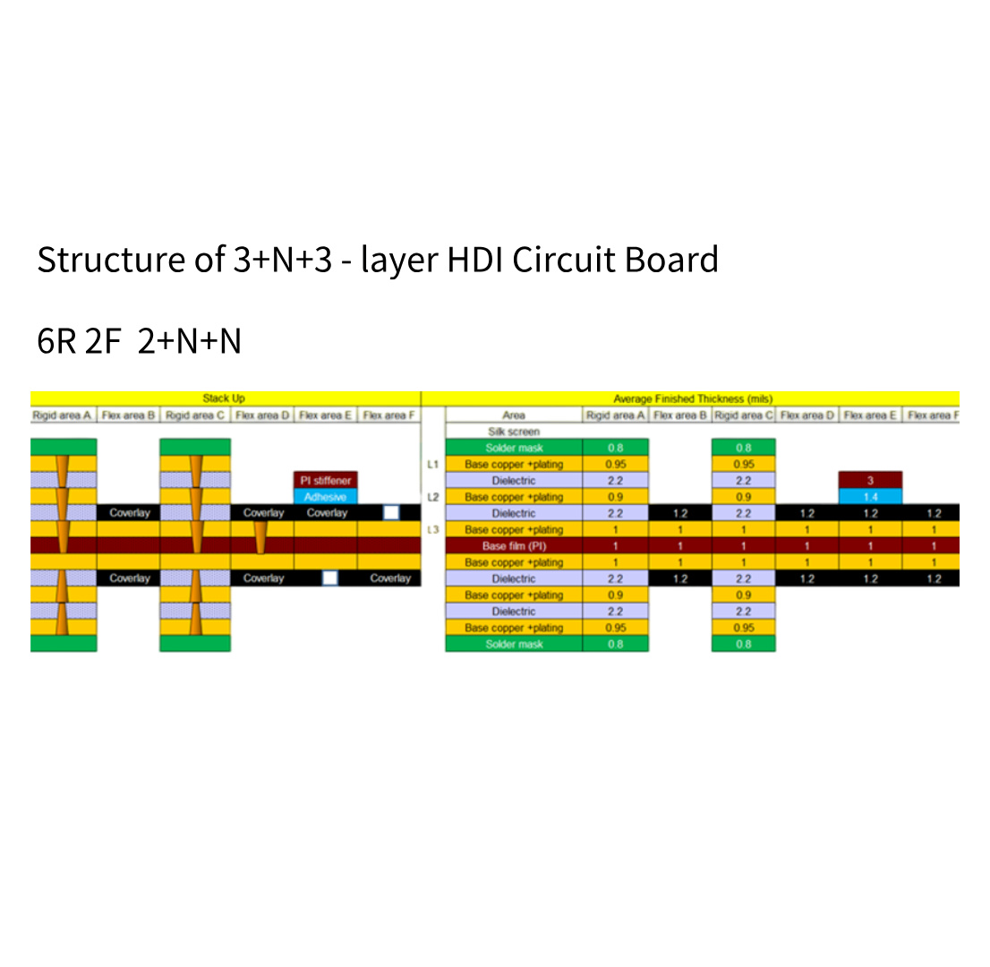
In the structure of the 3+N+3 - layer HDI circuit board, there are three rigid circuit - board layers on each side.
These three rigid circuit - board layers cooperate with each other to provide strong physical support and a stable foundation for electrical connections.
The outermost rigid layer can be used to install various electronic components. With its good mechanical properties, it can effectively protect the internal circuits from external physical damage.
The middle rigid layer plays a key role in signal transmission and power distribution, providing necessary connection paths for circuits in different functional areas.
The “N” layers in the middle are flexible circuit - board layers, and the value of “N” can be flexibly determined according to actual circuit design and performance requirements.
These flexible layers endow the circuit board with excellent bendability and flexibility, which can meet the needs of some special space layouts.
For example, in some scenarios where the circuit board needs to be bent into a specific shape to adapt to the complex space inside the device, the flexible layer plays a great role.
It can skillfully achieve the deformation of the circuit board without affecting the normal operation of the circuit.
At the same time, the flexible layer also helps to reduce the weight of the entire circuit board, which is an important advantage for weight - sensitive electronic devices.
Overall, the 3+N+3 - layer HDI circuit - board structure combines the stability of rigid circuit boards and the flexibility of flexible circuit boards. By reasonably designing the number of rigid and flexible layers and their respective functions, it can meet the diverse and high - performance electronic - circuit requirements and is widely used in fields such as high - end smartphones, tablets, and some industrial control devices with extremely high requirements for space utilization and circuit performance.
From the perspective of industry applications, the design and manufacturing of 3+N+3 - layer HDI circuit boards need to fully consider the special requirements of different industries.For example, in the industrial control field, the circuit board is required to have a strong anti - interference ability. Shenzhen Rich Full Joy Electronics Co., Ltd. effectively reduces the impact of electromagnetic interference on the performance of the circuit board by optimizing the circuit layout and using shielding materials.
In the aerospace field, extremely high requirements are put forward for the lightweight and high - temperature resistance of the circuit board. We adopt advanced materials and manufacturing processes. On the premise of ensuring the structural strength of the circuit board, we reduce the weight as much as possible and improve its high - temperature resistance to ensure the normal operation of the equipment in extreme environments.
When manufacturing 3+N+3 - layer HDI circuit boards, the inner - layer circuit manufacturing needs to take into account the circuit characteristics of different rigid and flexible layers and carry out refined processing.The lamination process is more complex and requires multiple high - temperature and high - pressure laminations. The parameters of each lamination are precisely controlled to ensure the close bonding between layers and the stability of the overall structure.
In the drilling and copper - plating process, for different types of holes (such as deep holes penetrating multiple rigid layers and transition holes connecting rigid and flexible layers), special drilling equipment and copper - plating processes are used to ensure the quality of the holes and the reliability of the copper - plating layer.
In the surface treatment stage, according to the special requirements of different application scenarios such as industrial control or aerospace, appropriate protective and solderability treatment methods are selected. For example, in the aerospace field, surface treatment processes with high and low - temperature resistance and radiation resistance may be more preferred.Key quality - control points (specific to the 3+N+3 - layer structure): For circuit boards applied in the industrial control field, electromagnetic compatibility (EMC) tests are carried out to ensure that the circuit board can work normally in a complex electromagnetic environment.
For circuit boards in the aerospace field, in addition to regular performance tests, high - low temperature cycle tests, radiation tests, etc. are also carried out to simulate the actual working environment and verify the reliability of the circuit board under extreme conditions.
During the lamination process, the pressure and temperature distribution are optimized according to the characteristics of multiple rigid layers to prevent delamination caused by inter - layer stress concentration.It should be emphasized that in the above three types, the number of Flex PCB layers represented by “N” is not fixed. Instead, according to specific design requirements, the professional engineer team of Shenzhen Rich Full Joy Electronics Co., Ltd. can use advanced design software and rich practical experience to carry out precise design and optimization adjustments to achieve the best balance between performance and cost.
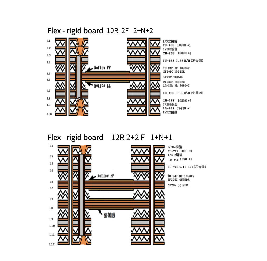
Structure of 10+N+10 - layer HDI Circuit Board
This type of HDI circuit board represents a further step up in terms of structural complexity and stability.
It consists of two layers of Rigid PCBs as the outermost layers, with multiple layers of Flex PCBs sandwiched in the middle.
This structural design significantly enhances the rigidity of the circuit board, enabling it to withstand greater external impacts and vibrations while retaining the bendable characteristics of the flexible circuit board.
In the motherboard design of high - end smartphones, the 10+N+10 - layer HDI circuit board plays a crucial role.
The internal space of a smartphone is extremely compact, requiring the circuit board to achieve complex functional integration and high - density wiring within a limited space.
The rigid outer layers of the 10+N+10 - layer structure can stably support various electronic components such as chips, capacitors, and resistors, ensuring that during the daily use of the mobile phone, even if it is slightly bumped or vibrated, good electrical connections can be maintained.
The flexible layers in the middle can flexibly adjust the circuit routing according to the internal space layout of the mobile phone, achieving efficient connections between different functional modules, such as connecting the motherboard to components like the display and camera, ensuring the stability and reliability of signal transmission and bringing a smooth user experience.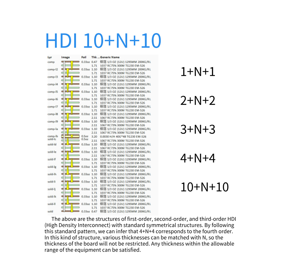
In the manufacturing process, for 10+N+10 - layer HDI circuit boards, the inter - layer alignment accuracy is one of the key factors affecting the performance of the circuit board.
Shenzhen Rich Full Joy Electronics Co., LtShenzhen Rich Full Joy Electronics Co., Ltd. uses an advanced optical positioning system to accurately align each layer before lamination to ensure the accurate connection of each layer of circuits.At the same time, in the transition area between the flexible layer and the rigid layer, we adopt special stress - buffering designs and material - processing techniques to effectively reduce the stress concentration problem caused by the differences in material properties and improve the long - term reliability of the circuit board。
With the continuous increase in the requirements for data transmission speed of modern electronic devices, high - speed signal transmission HDI circuit boards have become the key technology to meet this demand.In the production process, after the inner - layer circuits are made, multiple lamination operations are carried out. The uniformity of pressure and temperature is strictly controlled for each lamination to ensure the tight combination of the multi - layer structure.
In the drilling process, different drilling strategies and equipment parameters are adopted for holes in different positions (such as between rigid layers, between rigid and flexible layers, etc.) to ensure the positional accuracy and quality of the holes.
During the copper - plating process, the detection of the bonding strength of the copper - plating layer between different layers is strengthened to ensure the reliability of electrical connections.
Key quality - control points (specific to the 10+N+10 - layer structure): During multiple lamination processes, X - ray inspection is carried out after each lamination to check the inter - layer alignment and adjust the subsequent lamination parameters in a timely manner.
For the transition holes connecting the rigid and flexible layers, a special hole - wall treatment process is adopted after drilling to enhance the bonding force between the hole wall, the copper - plating layer, and different material layers.
The finished circuit board is subjected to vibration tests by simulating the vibration environment during mobile phone use to check the reliability of the connections of electronic components between different layers.
- HDI Structures: Symmetrical, Asymmetrical and Arbitrary Interconnection
- Symmetrical HDI Structures
- Standard Hierarchical Representation
The structure of first - order HDI is 1+N+1 layers.
The structure of second - order HDI is 2+N+2 layers.
The structure of third - order HDI is 3+N+3 layers.
The structure of fourth - order HDI is 4+N+4 layers.
The structure of tenth - order HDI is 10+N+10 layers
- Thickness Advantage
These are the standard symmetrical structures of HDI. By following this pattern, we can easily determine the hierarchical order. For example, the 4+N+4 structure is the fourth - order. In this type of structure, the value of N can be adjusted to match various thicknesses. As a result, the thickness of the circuit board is not restricted, and any thickness within the allowable range of the manufacturing equipment can be achieved.
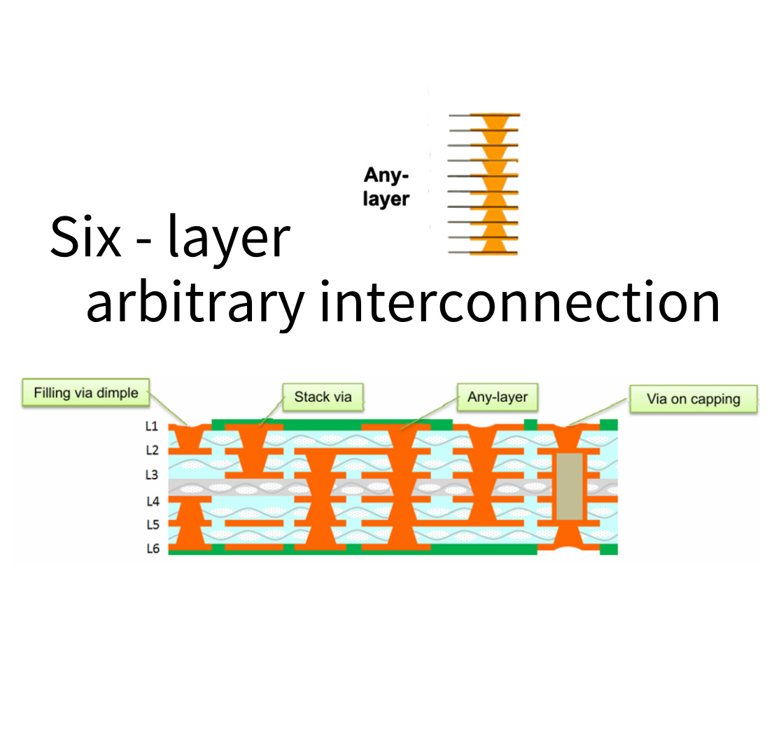
HDI - Arbitrary Interconnection HDI
- Concept Explanation
Arbitrary interconnection means that blind vias are required between each layer. For a 10 - layer circuit board, its structure can be represented as 1+1+1+1+1+1+1+1+1+1.
Thickness Limitation
Since blind vias are required for all layers, the thickness of each layer cannot exceed 0.1 millimeter. There are strict requirements for the thickness of the circuit board. If the thickness of each layer exceeds 0.1 millimeter, it is theoretically difficult to meet the design requirements.
Asymmetrical and Irregular HDI Structures
In addition to the above - mentioned standard symmetrical structures, there are many asymmetrical and irregular HDI structures. For example, structures like 2+N+4, 4+6, 5+8. As shown in the figure, it demonstrates a 14+2+7 asymmetrical structure. These non - standard structures are designed to meet the specific requirements in different applications. Although they are more complex in design and manufacturing compared to the standard symmetrical structures.
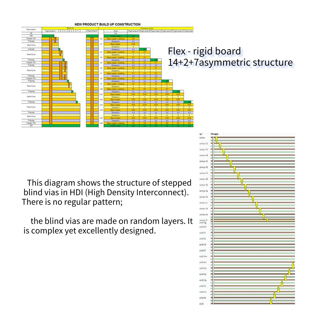
Regarding the naming of HDI, there are several common expressions. The full form is such as "High - Density Interconnect". In the electronics industry, HDI, as an abbreviation, is widely recognized and used. Sometimes, when emphasizing the technical aspect, it may also be referred to as "High - Density Interconnect Technology". However, the abbreviation "HDI" is by far the most commonly used and well - known term in technical documents and industry exchanges.
II. Special Types of HDI Circuit Boards
High - Order HDI Circuit Boards
High - order HDI circuit boards represent the top - level of HDI technology, a perfect combination of complex technology and precision manufacturing. It adopts more layers and extremely complex and sophisticated interconnection structures, just like constructing a criss - cross and highly efficient super - city traffic network in the micro - world.
Through this extreme design, high - order HDI circuit boards achieve ultra - high circuit density, can integrate a large number of electronic components in a very small space, and further reduce the overall size of the circuit board.
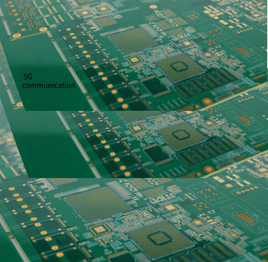
In fields with extremely demanding requirements for the performance of electronic devices, such as 5G communication base station equipment and high - performance computing servers, high - order HDI circuit boards play an irreplaceable core role.
Taking 5G communication base stations as an example, they need to handle massive data traffic and have extremely high requirements for the speed, stability, and accuracy of signal transmission. Through high - density wiring and optimized interconnection structures, high - order HDI circuit boards can achieve efficient transmission of high - speed signals between different functional modules, ensuring that base station equipment can quickly and accurately receive and send signals to meet the communication requirements of 5G networks with low latency and high bandwidth.
In high - performance computing servers, high - order HDI circuit boards can provide high - speed and stable signal connections for core chips such as CPUs and GPUs, support large - scale data operations and processing, and improve the overall performance and operating efficiency of the server.
From a technology R & D perspective, the manufacturing of high - order HDI circuit boards faces many challenges. For example, as the number of layers increases, the problem of inter - layer signal interference becomes more prominent. Shenzhen Rich Full Joy Electronics Co., Ltd. invests a large amount of R & D resources. By adopting advanced signal isolation technologies, optimizing the stack - up structure, and using low - loss materials, it effectively solves the inter - layer interference problem and ensures the quality of signal transmission.
At the same time, in the production of micro - holes and the processing of high - precision circuits, we continuously improve the process level. By using advanced laser processing equipment and precision etching technology, we achieve higher - precision circuit production and smaller - hole processing, meeting the requirements of high - order HDI circuit boards for miniaturization and high performance.
When manufacturing high - order HDI circuit boards, the production of inner - layer circuits requires extremely high precision. Advanced lithography technology and high - resolution photomasks are used to ensure the fineness and accuracy of the circuits.
During the lamination process, in order to ensure the tight combination of the multi - layer structure and the signal transmission performance, the control accuracy of temperature, pressure, and time is required to be extremely high. At the same time, special inter - layer insulating materials are used to reduce inter - layer capacitance and inductance and reduce signal interference.
In the drilling process, high - precision laser drilling technology is widely used to create micro - holes to meet the needs of high - density interconnection. After drilling, strict hole - wall treatment is carried out to ensure the good bonding between the copper - plating layer and the hole wall.
Advanced pulse electroplating technology is used in the copper - plating process to improve the uniformity and quality of the copper - plating layer and ensure the reliability of electrical connections.
Key quality - control points (specific to high - order HDI): Before lamination, a comprehensive impedance test is carried out on each layer of the circuit board to ensure that the inter - layer impedance matching meets the design requirements and reduces signal reflection and interference.
After drilling, high - end equipment such as atomic force microscopes is used to microscopically inspect the micro - hole walls to ensure that the hole - wall roughness meets the signal transmission requirements. Through high - speed signal transmission simulation tests, the signal integrity of the circuit board in actual high - speed data transmission scenarios is verified, and in - depth analysis and improvement are carried out on products with signal distortion.
Rigid - Flexible Combined HDI Circuit Boards
Rigid - flexible combined HDI circuit boards skillfully integrate the advantages of rigid and flexible circuit boards and are a highly innovative circuit - board design. The rigid part provides stable support and reliable electrical connections for the circuit board, ensuring that key electronic components can be stably installed and the signal transmission is stable. The flexible part endows the circuit board with excellent flexibility and bendability, enabling it to adapt to various special space layouts and usage scenarios.
In the field of foldable smartphones, the application of rigid - flexible combined HDI circuit boards has brought new breakthroughs in product innovation.
During the unfolding and folding of foldable smartphones, the circuit board needs to withstand repeated bending deformations while ensuring the stability of electrical connections. The rigid part of the rigid - flexible combined HDI circuit board can be used to carry key components such as the phone's core processor and storage chips, ensuring the normal operation of the phone's computing and storage functions. The flexible part can achieve smooth circuit connections at the screen folding point. As the screen opens and closes, the flexible circuit board can bend flexibly, ensuring the stable transmission of screen display signals and bringing users a seamless folding and unfolding experience.
In addition, in some medical device fields, such as wearable medical monitoring devices, the rigid - flexible combined HDI circuit boards can be fitted to the shapes of different parts of the human body to achieve accurate collection and transmission of physiological signals, while ensuring the comfort and reliability of the device.
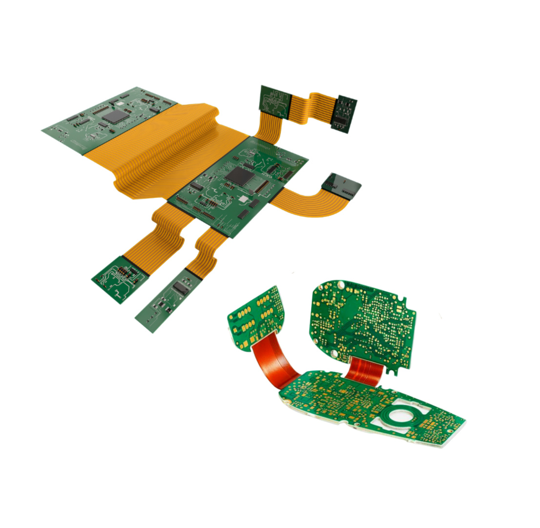
In terms of manufacturing process, the key to rigid - flexible combined HDI circuit boards lies in the transition connection between the rigid and flexible parts. Shenzhen Rich Full Joy Electronics Co., Ltd. adopts a unique integrated design and manufacturing process. At the junction of the rigid and flexible parts, through special material treatment and structural design, a smooth transition is achieved, effectively reducing stress concentration and improving the reliability of the circuit board during repeated bending.
At the same time, we use advanced flexible circuit manufacturing technology to ensure that the circuits in the flexible part have good flexibility and electrical performance and can withstand long - term bending and stretching tests.
When manufacturing rigid - flexible combined HDI circuit boards, the inner - layer circuit production is optimized for the rigid and flexible parts respectively. The rigid part focuses on the load - bearing capacity and stability of the circuits, while the flexible part focuses on the flexibility and bendability of the circuits.
During the lamination process, the lamination process for the transition area between the rigid and flexible parts is specially designed. Special prepregs and lamination parameters are used to ensure the bonding strength and flexibility of the transition area.
In the drilling and copper - plating process, special drilling and copper - plating processes are used for the holes in the transition area between the rigid and flexible parts to ensure the quality of the hole wall and the adhesion of the copper - plating layer to adapt to the stress changes during the bending process.
Key quality - control points (specific to rigid - flexible combined HDI): After the inner - layer circuits in the transition area between the rigid and flexible parts are completed, a high - precision scanning electron microscope is used to check the connection reliability and edge quality of the circuits to ensure there are no hidden dangers of open circuits or short circuits.
During the lamination process, local pressure monitoring is carried out on the transition area to ensure uniform pressure distribution and avoid poor bonding due to uneven pressure.
After the circuit board is assembled, a simulated folding test is carried out for no less than [X] times. During this period, the electrical performance is monitored in real - time to check whether the signal transmission is stable. The number and location of failures are recorded, and the causes are analyzed and improved.
A tensile test is carried out on the circuits in the flexible part to simulate the stretching scenarios in daily use, ensuring that the circuits can still maintain good electrical connections and mechanical properties under tension.
High - Speed Signal Transmission HDI Circuit Boards
During the design and manufacturing process of this type of circuit board, a series of special materials and advanced processes are adopted to minimize signal distortion and interference during transmission.
For example, in material selection, we choose boards with low dielectric constant and low loss to reduce energy loss and delay during signal transmission.
In terms of circuit layout, impedance matching is achieved by optimizing the circuit routing, controlling the circuit length and spacing, ensuring that high - speed signals can be transmitted with minimal loss and interference.
In fields such as high - speed network communication equipment and high - definition video transmission equipment, high - speed signal transmission HDI circuit boards play a crucial role.
In high - speed network communication equipment such as routers and switches, high - speed signal transmission HDI circuit boards can ensure the fast and accurate transmission of data in high - speed networks, reducing signal delay and packet loss, and providing users with a stable and smooth network connection.
In high - definition video transmission equipment such as 4K/8K video playback devices and video surveillance systems, high - speed signal transmission HDI circuit boards can ensure the high - quality transmission of high - definition video signals, avoiding problems such as picture freezing and screen distortion, and bringing users an ultimate visual experience.
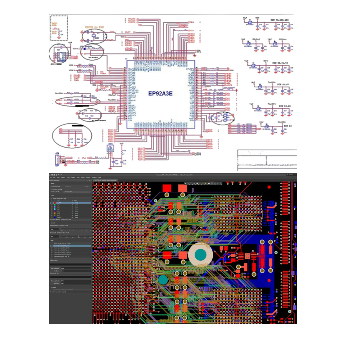
From the perspective of industry development trends, with the rapid development of emerging technologies such as 5G communication, the Internet of Things, and artificial intelligence, the demand for high - speed signal transmission HDI circuit boards will continue to grow. Shenzhen Rich Full Joy Electronics Co., Ltd. will closely monitor industry trends, continuously increase R & D investment, and continuously optimize the design and manufacturing processes of high - speed signal transmission HDI circuit boards to meet the ever - increasing market demand for high - speed and stable data transmission.
When manufacturing high - speed signal transmission HDI circuit boards, the inner - layer circuit production focuses on optimizing the circuit layout to reduce interference sources on the signal transmission path. Low - dielectric - constant prepregs and copper foils are selected for lamination to reduce signal transmission losses. During the drilling and copper - plating process, the dimensional accuracy of the holes and the uniformity of the copper - plating layer are strictly controlled to minimize the impact on signal transmission. High - precision etching technology is used for outer - layer circuit production to ensure the flatness and edge quality of the circuits and avoid signal reflection. For surface treatment, processes with little impact on signal transmission, such as organic solderability preservative (OSP), are selected. While ensuring solderability, the interference with high - speed signals is minimized.
Key quality - control points (specific to high - speed signal transmission HDI): In the raw material inspection stage, the dielectric properties of low - dielectric - constant boards are accurately tested to ensure compliance with high - speed signal transmission requirements. Professional signal integrity analysis software is used to simulate and verify the circuit layout design, and potential signal interference problems are detected and solved in a timely manner before production. After drilling and copper - plating, a high - precision impedance tester is used to measure the line impedance point by point to ensure that the impedance matching accuracy is within a very small error range. The finished circuit board is subjected to high - speed signal transmission tests, simulating the highest rates and complex signal environments in actual applications. Signal quality is evaluated through means such as eye - diagram analysis, and substandard products are strictly prohibited from leaving the factory.
- III. Overview of HDI Circuit Board Production Process and Key Quality - Control Points
The production of HDI circuit boards is a highly precise and complex process involving numerous advanced technologies and strict process controls. It mainly includes the following key steps and corresponding quality - control points:
- Inner - Layer Circuit Production
First, prepare the copper - clad laminate. The designed circuit pattern is transferred onto the copper plate through lithography technology, and the unnecessary copper layer is removed by etching process to form accurate inner - layer circuits. This step requires high - precision lithography equipment and precise etching control to ensure the fineness and accuracy of the circuits.
Key quality - control points: Before lithography, the photomask is strictly inspected to ensure that the pattern has no defects and is highly clear. During lithography, parameters such as exposure intensity and time are monitored in real - time to ensure the accuracy of circuit transfer. During etching, the concentration, temperature, and etching time of the etchant are strictly controlled. The etching rate is monitored in real - time through on - line detection equipment to prevent over - etching or under - etching of the circuits and ensure that the circuit width and spacing meet the design requirements.
- Lamination
The fabricated inner - layer circuit boards, prepregs, and outer - layer copper foils are stacked according to the design requirements and placed in a high - temperature and high - pressure laminator. Under precisely controlled temperature, pressure, and time conditions, the prepregs melt and firmly bond the layers together to form the basic structure of the multi - layer board. The lamination process has extremely high requirements for the temperature uniformity and pressure stability of the equipment to ensure tight inter - layer bonding and no defects such as bubbles and delamination.
Key quality - control points: Before lamination, the surface quality of the inner - layer circuit boards, prepregs, and outer - layer copper foils is carefully inspected to ensure there are no impurities, scratches, and other problems. The temperature sensors and pressure sensors of the laminator are strictly calibrated to ensure the accuracy and uniformity of temperature and pressure. After lamination, X - ray inspection equipment is used to check for defects such as bubbles and delamination between layers, and defective products are promptly reworked or scrapped.
- Drilling and Copper - Plating
High - precision drilling equipment such as laser drilling machines is used to drill micro - holes, blind holes, and buried holes for connecting the circuits of each layer. Subsequently, electroless copper plating and electroplating are carried out to deposit a uniform layer of copper on the hole wall, ensuring good electrical connections between the circuits of each layer. During the copper - plating process, parameters such as the composition of the plating solution, temperature, and current density are strictly controlled to ensure the thickness and quality of the copper layer.
Key quality - control points: Before drilling, the drilling equipment is calibrated for accuracy to ensure accurate drilling positions. During the drilling process, parameters such as drilling depth and hole diameter are monitored in real - time to prevent problems such as drilling deviation and through - drilling. During copper - plating, the composition of the plating solution is regularly tested, and the performance of the plating solution is monitored through methods such as Hull cell tests to ensure uniform copper layer thickness and strong adhesion. Means such as metallographic section analysis are used to check the quality of the copper layer on the hole wall, such as the presence of voids and looseness.
- Outer - Layer Circuit Production
The lithography and etching processes are used again to produce the outer - layer circuits on the laminated board. The process is similar to that of inner - layer circuit production, but the accuracy and reliability requirements for the outer - layer circuits are higher to meet the needs of high - density wiring.
Key quality - control points: Similar to inner - layer circuit production, strict quality control is carried out on the photomask for outer - layer circuit lithography. During lithography and etching, the inspection of circuit accuracy is strengthened. Equipment such as electron microscopes is used to spot - check the edge quality and line - width accuracy of the circuits to ensure compliance with design standards. After etching, the circuit surface is inspected for problems such as etching residues and short circuits.
- Surface Treatment
To prevent oxidation of the copper layer and enhance solderability, the surface of the circuit board is treated. Common methods include hot - air solder leveling (HASL), electroless nickel immersion gold (ENIG), organic solderability preservative (OSP), etc. Different surface treatment methods are suitable for different application scenarios, and the appropriate process needs to be selected according to product requirements.
Key quality - control points: Before surface treatment, ensure that the circuit board surface is clean and free of oil stains and impurities. For the hot - air solder leveling process, the temperature of the tin - lead alloy and the soldering immersion time are strictly controlled to ensure that the solder joints are flat and smooth, and there are no problems such as dry soldering and bridging. In the electroless nickel immersion gold process, the pH value, temperature, and plating time of the plating solution are precisely controlled to ensure uniform thickness of the nickel and gold layers. The surface treatment effect is verified through means such as solderability tests. For the organic solderability preservative process, the film thickness uniformity is controlled, and real - time monitoring is carried out through a film - thickness tester.
- Testing and Inspection
The circuit board is comprehensively tested through various testing methods such as electrical performance testing, X - ray inspection, and flying - probe testing to ensure that its performance indicators meet the design requirements. Only products that pass strict testing can enter the next step.
Key quality - control points: During electrical performance testing, test parameters are set according to standard specifications, and key indicators such as circuit board conductivity, insulation resistance, and impedance are accurately measured to ensure good signal transmission performance. X - ray inspection is used to check the internal inter - layer structure, hole quality, etc., and internal defects are detected in a timely manner. Flying - probe testing conducts point - to - point electrical connection tests on the small components and complex circuits on the circuit board to ensure the accuracy of circuit connections. For unqualified products, a detailed failure analysis is carried out, the root cause of the problem is traced, and corresponding improvement measures are taken.
- Forming and Post - Processing
According to the design dimensions, the circuit board is formed by mechanical processing or laser cutting. Finally, post - processing procedures such as cleaning and packaging are carried out to complete the production of the HDI circuit board.
Key quality - control points: During the forming process, the processing dimensional accuracy is strictly controlled. High - precision measuring equipment is used to spot - check the dimensions of the formed circuit board to ensure compliance with the design drawing requirements. In the cleaning process, ensure that the concentration, temperature, and cleaning time of the cleaning solution are appropriate to ensure that there are no residual impurities on the circuit board surface. When packaging, appropriate packaging materials and methods are used to prevent damage to the circuit board during transportation and storage.
Shenzhen Rich Full Joy Electronics Co., Ltd., with its profound technical foundation, rich industry experience, and professional engineering team, has a deep understanding of the unique key points and challenges in the design, manufacturing, and application of each type of HDI circuit board. We can accurately select the most suitable solution from a wide range of HDI circuit board types according to the specific application requirements of customers. Through advanced production processes, strict quality control, and continuous technological innovation, we create high - quality and high - performance HDI circuit board products for customers, helping them achieve greater success in the field of electronic device manufacturing.
In addition, with the continuous progress of science and technology and the continuous promotion of innovation, HDI circuit board technology is also advancing rapidly. Shenzhen Rich Full Joy Electronics Co., Ltd. will always maintain a keen market insight, actively engage in the research and exploration of new technologies, continuously expand the application boundaries of HDI circuit boards, inject an endless stream of impetus into the development of the electronic device manufacturing industry, and lead the industry to new heights.





















