











Multilayer High-Frequency PCB Manufacturing: Key Lamination Process Insights and Quality Control
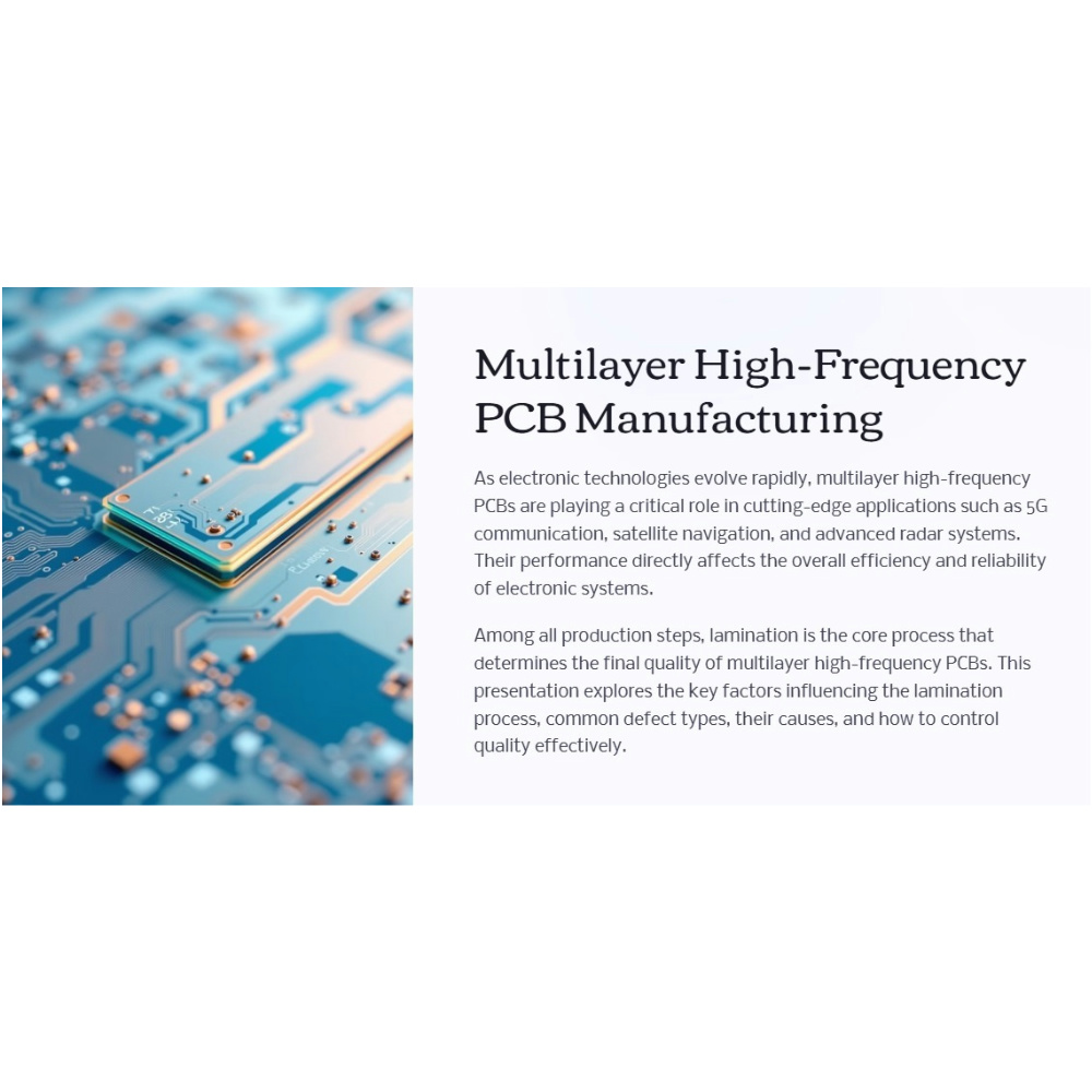
With the rapid advancement of electronics, multilayer high-frequency PCBs have become indispensable in cutting-edge applications such as 5G communication, satellite navigation, and radar systems. As signal frequencies increase, the quality of the lamination process becomes a decisive factor in achieving high performance, reliability, and long service life.
In this article, we explore the critical steps of multilayer high-frequency PCB lamination, examine common defect mechanisms, and highlight effective quality control measures for superior PCB manufacturing outcomes.
Lamination Process Essentials
1. Material Preparation
✔ Substrate Selection
High-frequency PCBs require materials with:
●Low dielectric constant (Dk): for faster signal propagation
●Low dissipation factor (Df): to minimize signal loss
Preferred substrates include Rogers and Taconic. For example, 5G base station PCBs typically use substrates with Dk values between 3.0–3.5, ensuring consistent performance across high-speed data channels.
✔ Copper Foil Characteristics
●Low surface roughness: reduces conductor loss
●High purity: ensures lower resistance and better signal transmission
Typical copper weights: 1/2 oz or 1/4 oz electrolytic copper, ideal for RF performance.
✔ Prepreg (PP) Compatibility
Prepregs serve as the adhesive layer in lamination. Key factors include:
●Resin content and flow: must match the base material and copper foil
●Different types of prepregs are used based on PCB thickness and layer count. Proper prepreg selection ensures strong interlayer adhesion and electrical performance.
2. Inner Layer Fabrication
✔ High-Precision Imaging & Etching
●Photoresist exposure must reach micron-level accuracy
●Etching uniformity is essential to maintain line width/space tolerance (e.g., 50μm/50μm)
✔ Inner Layer Inspection
Post-etching, rigorous inspection using AOI (Automated Optical Inspection) and flying probe testing ensures defect-free circuitry. Even minor shorts or opens can cause critical failures in high-frequency designs after lamination.
3. Lamination Execution
✔ Pre-Lamination (Pre-Pressing)
Objective: expel trapped air and volatiles
●Temperature: 60–80°C
●Pressure: 1–2 MPa
●Time: 5–10 min
Pre-pressing ensures initial layer adhesion and flattens material layers for optimal lamination results.
✔ Hot Press Lamination
Core process where prepreg resin flows and cures:
●Temperature: 180–220°C
●Pressure: 5–10 MPa
●Time: 30–60 min
●Hot plate temperature uniformity: ±2°C is crucial to avoid resin curing imbalance
Resin must evenly fill the spaces between layers to ensure strong adhesion and avoid voids.
✔ Controlled Cooling
●Ideal cooling rate: 1–3°C/min
●Prevents internal stress and warpage
Gradual cooling allows mechanical stress relief, ensuring dimensional stability and flatness.

Common Lamination Defects and Root Causes
Interlayer Delamination
Symptom:
●Visible or microscopic layer separation
●Reduced peel strength (< 1.5N/mm)
Causes:
●Moisture-contaminated or low-resin prepregs
●Insufficient lamination pressure or temperature
●Resin cure failure due to poor storage or excessive humidity
Impact:
●Signal attenuation and distortion
●Long-term reliability degradation
Internal Voids (Bubbles)
Symptom:
●Air pockets detected via X-ray inspection
●Ranges from pinhead-sized to millimeter-scale voids
Causes:
●Incomplete air evacuation during pre-press
●Rapid heating causes volatile outgassing
●Poor material degassing or prepreg selection
Impact:
●Unpredictable air-gap capacitance
●RF phase shift and increased insertion loss

PCB Warpage and Deformation
Symptom:
●PCB bends, twists; exceeds 0.5% flatness tolerance
●Difficulties in SMT assembly, mechanical misalignment
Causes:
●Uneven cooling post-lamination
●CTE mismatch across layers
●Unequal pressure or copper distribution
Impact:
●Cracked solder joints
●Line breaks under mechanical stress
●Reduced assembly yield and field reliability
Rich Full Joy’s Expertise in High-Frequency PCB Lamination
With deep industry experience in RF PCB manufacturing, Rich Full Joy understands the delicate balance required between material properties, thermal profiles, and process precision. Our key capabilities include:
●Expertise in Rogers, Taconic, and other advanced materials
●High-precision lamination temperature and pressure control systems
●Advanced X-ray, AOI, and peel-strength testing equipment
●Integrated design-for-manufacturing (DFM) support
We ensure that your multilayer high-frequency PCBs meet the stringent signal integrity and mechanical stability standards required for 5G, radar, satellite, and aerospace applications.
Partner With Rich Full Joy
If you're navigating the complexities of multilayer RF PCB lamination, Rich Full Joy is your ideal partner. Our proactive quality control, in-depth material knowledge, and tailored engineering solutions help you:
●Reduce defect rates
●Accelerate time to market
●Achieve unmatched RF performance
Contact us today or follow our technical updates—we're committed to powering the next generation of communication with world-class PCB solutions.









