











Common SMT Process Defects and Solutions: A Complete Guide for Reliable PCB Assembly
Why SMT Process Defect Control Is Critical
Surface Mount Technology (SMT) demands micron-level precision in paste deposition, component placement, and thermal management. Variations in stencil design, solder paste volume, or reflow profiles can induce defects that compromise product reliability—especially in high-density, high-speed, or multilayer designs. For aerospace, automotive, medical, and telecom applications, undetected SMT defects may cause catastrophic field failures. This guide details prevalent SMT defects, their root causes, and engineering solutions.
1. Tombstoning (Manhattan Effect)
Definition: A chip component (e.g., 0201/0402) lifts vertically during reflow, separating from one pad.
Technical Causes:
- ·Imbalanced solder paste volume between paired pads
- ·Asymmetric thermal mass (e.g., unequal trace widths or copper pour)
- ·Excessive reflow ramp rate (>2°C/sec)
- ·Non-optimized stencil aperture design
- ·Pad geometry violating IPC-7351 symmetry rules
Engineering Solutions:
- ·Design symmetric pads/traces per IPC-7351B guidelines
- ·Match stencil aperture sizes/volumes for component terminations
- ·Limit reflow ramp rate to 1–2°C/sec
- ·Apply aperture overprint (for ≤01005 passives)
- ·Avoid component placement near large copper planes
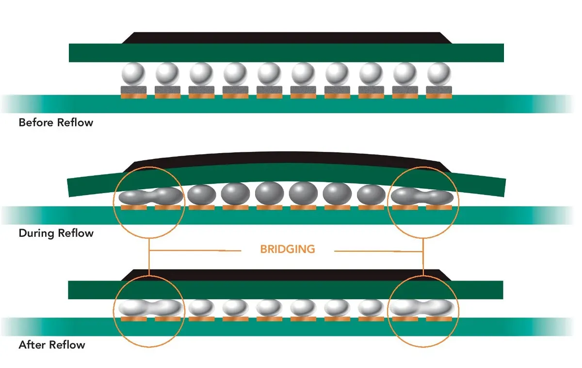
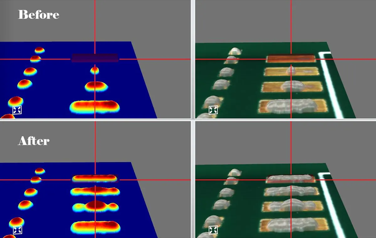
2. Solder Bridging
Definition: Unintended solder connection between adjacent conductors/pads.
Technical Causes:
- ·Oversized stencil apertures or excessive paste volume
- ·Insufficient solder mask dam (<0.05mm) for fine-pitch components (<0.4mm)
- ·Poor paste release (e.g., inadequate stencil aspect ratio)
- ·Misalignment during stencil printing
Engineering Solutions:
- ·Implement aperture reductions (e.g., “dog-bone” for QFPs, “home-plate” for BGAs)
- ·Optimize aperture aspect ratio (≥1.5) and area ratio (≥0.66)
- ·Specify solder mask dam width ≥0.025mm for fine-pitch designs
- ·Deploy 3D Solder Paste Inspection (SPI)
- ·Enforce stencil cleaning protocols
3. Insufficient Solder (Non-Wetting/Open Joints)
Definition: Incomplete metallurgical bond due to inadequate solder.
Technical Causes:
- ·Insufficient paste volume
- ·Suboptimal reflow profile (low peak temp or TAL)
- ·Pad/component oxidation
- ·Paste drying during extended exposure
Engineering Solutions:
- ·Reflow optimization: 240–245°C peak, 60–90s TAL
- ·Use Type 4/5 paste
- ·Specify ENIG/ENEPIG finishes
- ·Control printing environment: 25±3°C, 40–60% RH
4. Component Shift/Misalignment
Definition: Component displacement during reflow.
Technical Causes:
- ·Inadequate paste tack
- ·Conveyor vibration/convection issues
- ·Incorrect nozzle force/z-height
- ·PCB warpage near Tg
Engineering Solutions:
- ·Paste tack strength >500g/mm²
- ·Calibrate pick-and-place: ≤30μm accuracy, 0.2–0.5N force
- ·Control fan speed and conveyor vibration
- ·Use FR-4 Tg170+ or fixture support
5. Solder Joint Voids
Definition: Gas entrapment creating cavities in joints.
High-Risk Areas: QFN thermal pads, BGA balls, high-current vias.
Technical Causes:
- ·Rapid ramp trapping flux volatiles
- ·Moisture in unbaked MSL 2a+ components
- ·Via-in-pad without fill/capping
- ·Poor wetting behavior
Engineering Solutions:
- ·Ramp rate: 1.0–1.5°C/sec
- ·Pre-bake per J-STD-033
- ·Filled/capped vias
- ·Use vacuum reflow or low-voiding paste
6. Head-in-Pillow (HIP)
Definition: BGA ball contacts paste but fails to coalesce.
Technical Causes:
- ·Warpage mismatch
- ·Oxidized solder balls
- ·Too short TAL
Engineering Solutions:
- ·Bake BGAs: 125°C/12–24hr
- ·Use flux with ≥0.2% activity
- ·Extend TAL to >90s, verify with X-ray
- ·Optimize stackup for warpage control
7. Solder Ball Splatter
Definition: Micro-solder balls (<0.1mm) post-reflow.
Technical Causes:
- ·Aggressive ramp (>3°C/sec)
- ·Inconsistent alloy:flux paste
- ·Pad contamination
- ·Weak solder mask adhesion
Engineering Solutions:
- ·No-clean paste with stable resins
- ·Preheat ramp: 1.0–1.5°C/sec to 150–180°C
- ·Apply plasma cleaning
- ·Specify solder mask with CTI >175V
8. Pad Lifting/Delamination
Definition: Pad separation from PCB base.
Technical Causes:
- ·Excessive rework cycles
- ·Low z-axis CTE or Tg material
- ·Moisture absorption
Engineering Solutions:
- ·Limit to ≤2 heat cycles per pad
- ·Use thermocouple-controlled rework tools
- ·Bake PCBs: 125°C/4–8hr (IPC-1601)
- ·Use laminates: Tg >170°C, Td >340°C
Systematic SMT Defect Prevention
- ·DFM: IPC-2581, IPC-7351B land pattern checks
- ·Inspection: Inline SPI → AOI → AXI, KIC oven profiling
- ·Material: MSL per IPC-J-STD-033, SLP testing
- ·Training: IPC-A-610H, IPC-7711/7721 certification
Achieve Zero-Defect SMT with Rich Full Joy
Reliable SMT requires mastery of material-process-design interactions. At Rich Full Joy, we deliver mission-critical PCBA through:
- ·Process-Optimized DFM: Real-time feedback with Valor NPI
- ·Advanced Inspection: 3D SPI, AI-powered AOI, 5μm X-ray
- ·High-Reliability Assembly: μBGA (0.2mm), QFN voiding <10%
- ·Traceability: Component-level genealogy logging
Contact us for a complimentary DFM review and SMT process audit.









