











The Importance of High-Frequency PCBs in Electronics Manufacturing
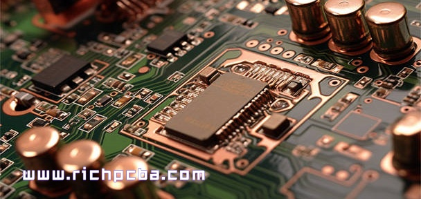
As electronics continue to advance in complexity and demand faster signal transmission rates, high-frequency PCBs have become a crucial component in the development of high-performance applications across the manufacturing sector.
High-frequency printed circuit boards (PCBs) have become indispensable in electronics manufacturing, offering a range of essential features. In essence, high-frequency PCBs efficiently transmit electromagnetic waves with minimal loss and ensure high-speed signal flow. Key properties associated with high-frequency PCBs include:
Low Dissipation Factor: High-frequency PCBs typically exhibit a dissipation factor ranging from 0.0019 to 0.025, ensuring minimal signal loss and maintaining signal transmission rates.
Low Dielectric Constant: These PCBs feature a low and stable dielectric constant, facilitating smooth frequency transmission and minimizing signal delay.
Chemical Resistance: The ability of high-frequency PCBs to withstand exposure to chemicals is highly valuable, ensuring resistance to corrosion and suitability for environments with significant chemical exposure.
Low Moisture Absorption: With a low rate of water absorption, high-frequency PCBs are well-suited for use in damp and humid environments.
Low Dimensional Stability: High-frequency PCBs are recognized for maintaining their size and remaining unaffected by environmental temperature changes.
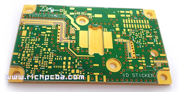
Given these characteristics, their application is widespread. However, PCB designers must ensure that the following steps are meticulously followed when designing high-frequency PCBs:
Determine the PCB signal frequency: It is crucial to establish the voltage and power requirements, divide any power planes, and assess the accommodation of different signals. Additionally, minimizing tolerance levels and reducing noise levels are important considerations.
Board stackup planning: The requirements for the stackup layer must be carefully planned, taking into account the specific material and its limitations.
Floor planning: The PCB should be divided into sections, with proper isolation maintained in areas containing digital and analog sections to prevent interference.
Power and ground planes: Once the PCB layout is defined, understanding the ground plan is essential. Dividing the ground plane is imperative, and including a resistor along with the signal trace to enhance the return path is crucial.
Reduce the size of land patterns: High-frequency PCBs often feature small pads. Shrinking the space helps minimize parasitic capacitance and increases mechanical strength.
Route the frequency signals: High-frequency signals are known to produce high radiation. Effective routing of the frequency signals can prevent interference between signals.
Use the 3W rule: Adhering to the 3W rule ensures that signal integrity is maintained, establishing a difference between traces and minimizing the coupling effect.
Apply the 20H rule: Coupling between ground and power planes can pose a threat to your design. The 20H rule ensures that the thickness between adjacent power and ground planes is greater than the power plane.
Utilization of High-Frequency PCBs
The use of high-frequency PCBs is increasingly prevalent, with applications including:
Communication systems in filtering devices, amplifiers, booster stations, and receivers.
Military applications for the production of ammunition and firearms.
Radar systems that guide aircraft and prevent accidents.
Mission-critical diagnostic and monitoring devices in the medical industry.
In Conclusion
High-frequency PCBs are essential in electronics PCB manufacturing, offering robust features that make them a preferred choice for electronic appliances. They play a significant role in high-performance applications and are poised to become even more crucial with the growing complexity of electronics and the demand for faster signal transmission rates.









