




0102030405
News

How to Choose a PCB Manufacturer
2024-07-15
From a Product Perspective:
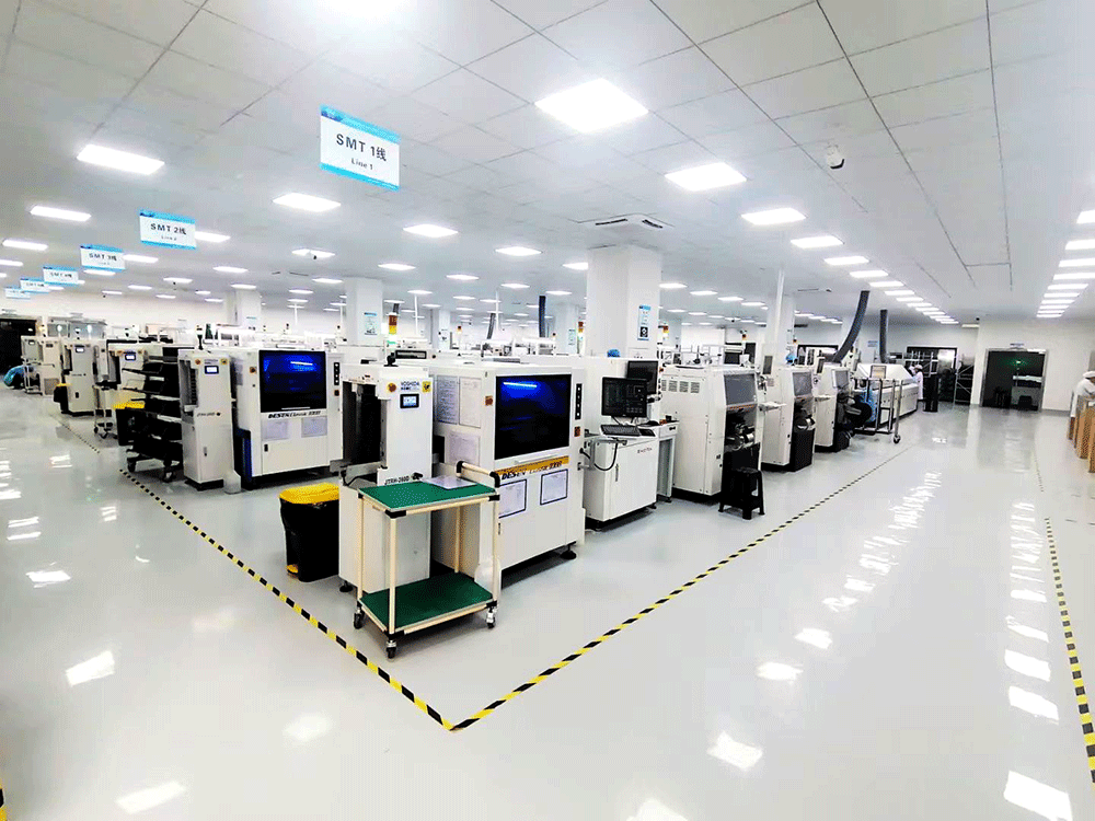
PCB manufacturers can provide free product samples. Customers can arrange visits to the factory or obtain samples from the company. By inspecting the samples or consulting someone knowledgeable about PCBs, they can preliminar...
view
detail
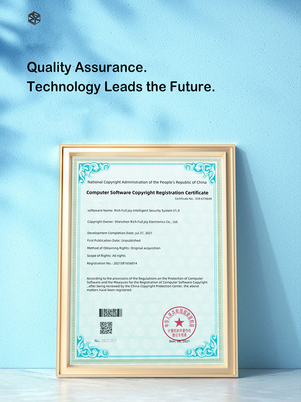
Good news | Received Patent for Rich Full Joy Intelligent Security System V1.0
2021-10-13
With the continuous acceleration of urbanization, the size and population density of cities are constantly increasing, and cities are facing more and more security challenges and threats. Traditional security systems require a large amount of manpower and mate...
view
detail
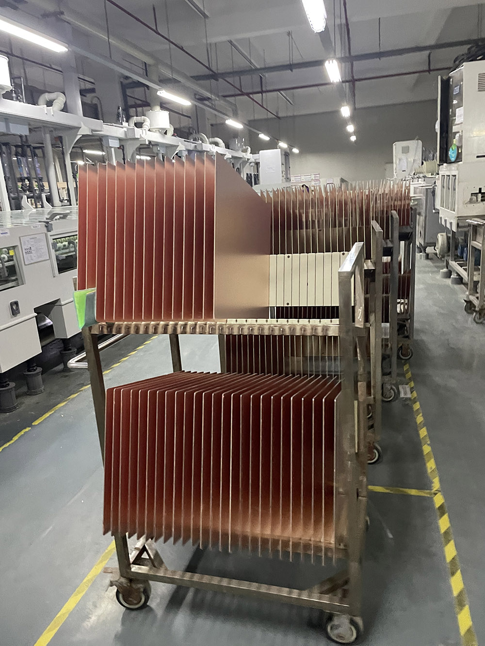
How to Manufacture High-Quality PCBs? Comprehensive Guide to Key PCB Manufacturing Steps
2020-04-25
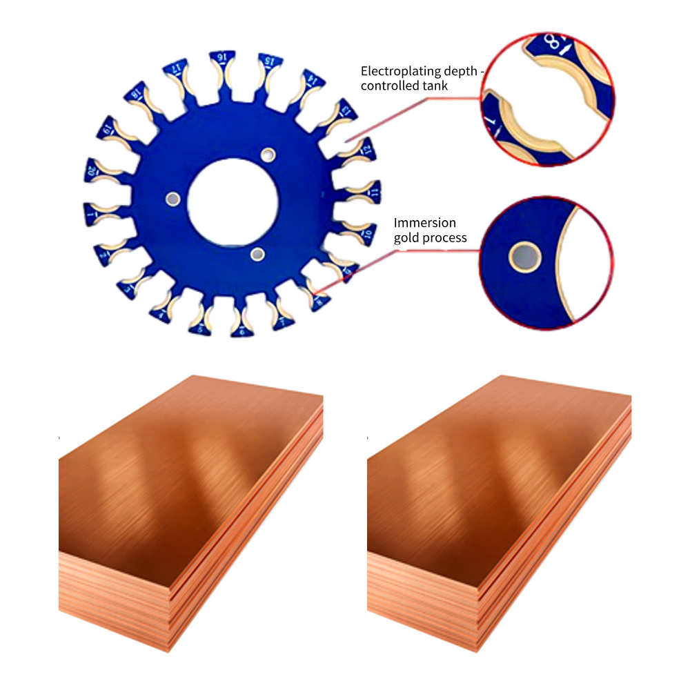
The PCB production process encompasses several key steps, starting from verifying the board-making data provided by suppliers, including material cutting, drilling, chemical copper sinking, image transfer, graphic plating, film removal, etching, solder mask application, silkscreen printing, gold fingers coating, forming, and final testing. Each step is rigorously executed according to process requirements to ensure the quality and precision of the circuit boards. Through these steps, PCB manufacturers can produce high-quality, fully functional printed circuit boards to meet a wide range of electronic product requirements.
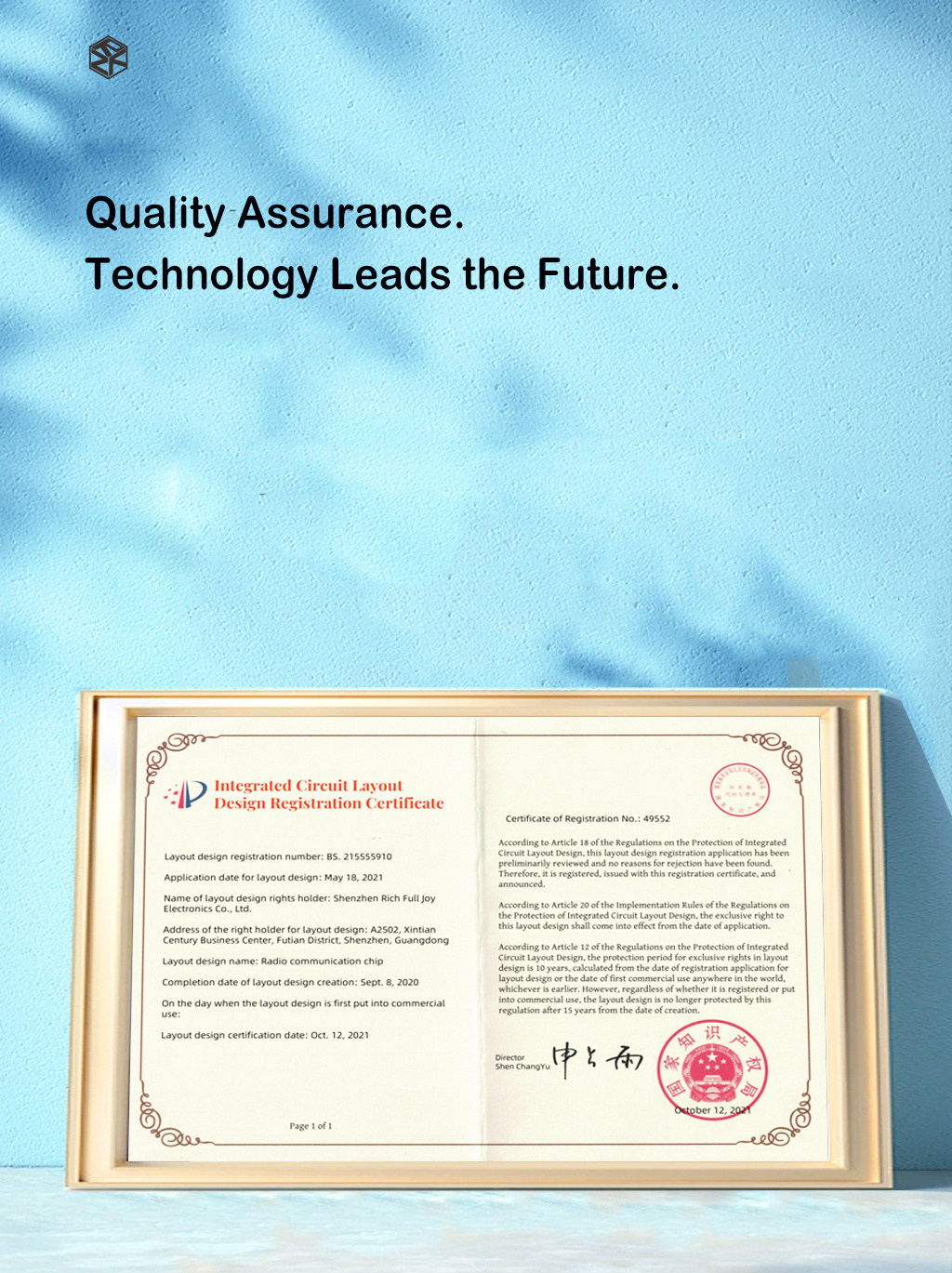
Good news | Received patent for wireless communication chip
2021-10-13
With the rapid development of wireless communication technology, the importance of wireless communication chips as the core component of wireless communication systems is becoming increasingly prominent. Traditional wireless communication chips often have fixe...
view
detail
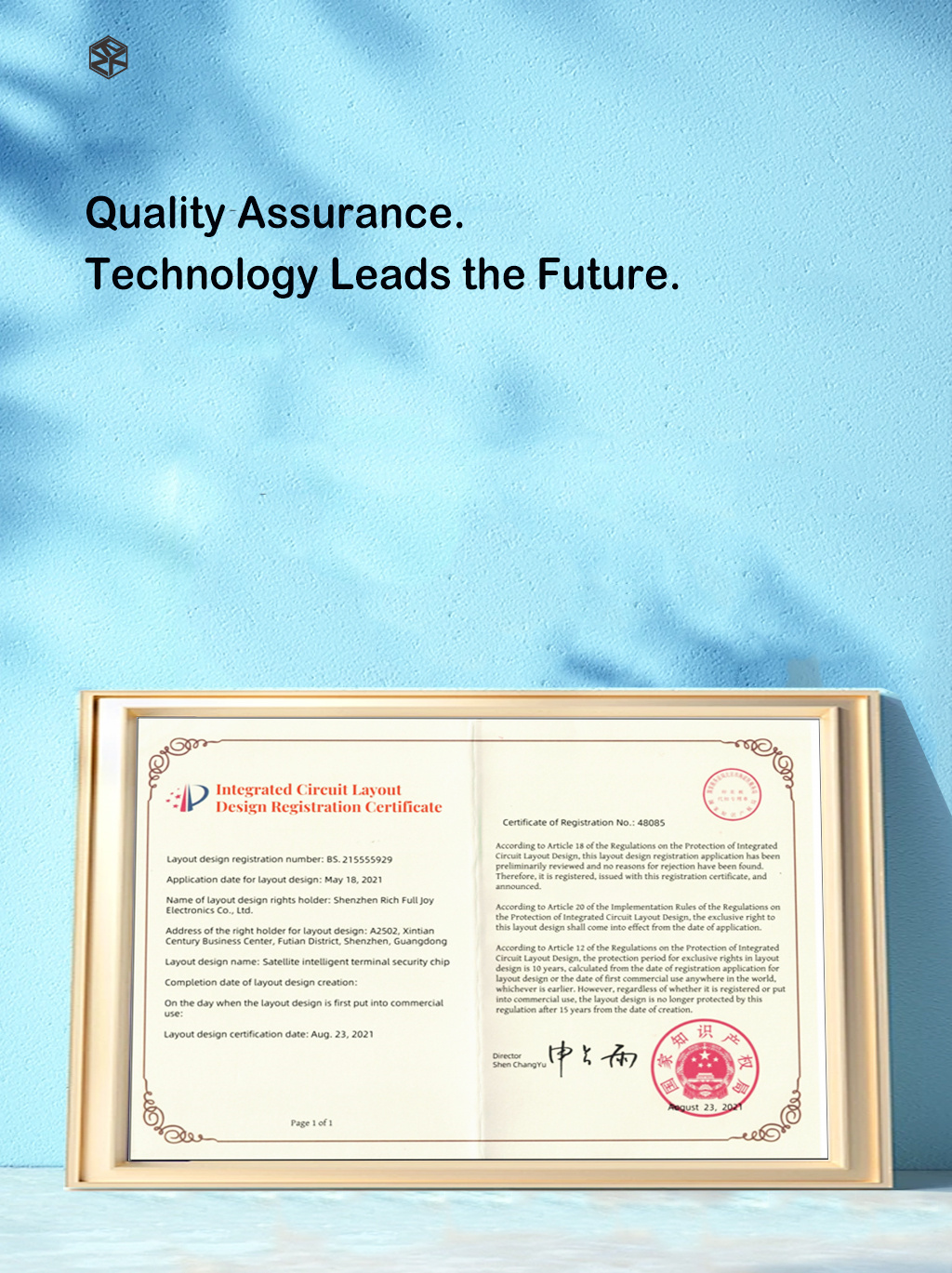
Good news | Received patent for Satellite Intelligent Terminal Security Chip
2021-08-24
In today's rapidly developing world, satellite intelligent terminal security chips have emerged, aiming to solve security problems through innovative points. With the continuous development of network technology, network security issues are becoming increasing...
view
detail
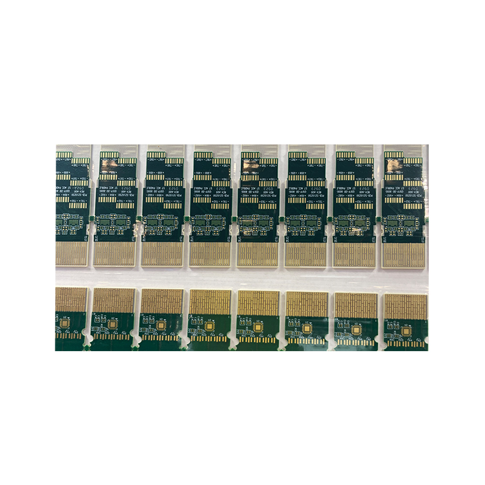
PCB Gold Finger Design and Processing Guide
2021-07-21
Gold Finger PCB is a special type of printed circuit board, commonly used in applications that require high reliability and wear resistance, such as computer motherboards, graphics cards and other electronic devices. This article will delve into the definition...
view
detail
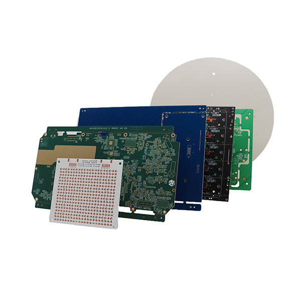
Do you know the function of PCB solder mask? What are the options for PCB solder mask?
2020-05-08
IPC has established a solder mask testing standard as an industry guide for material manufacturers, OEMs, and PCB manufacturers. IPC SM-840D classifies solder mask layers, Class T and Class H, summarized as follows:T-Telecommunications: including computers, te...
view
detail
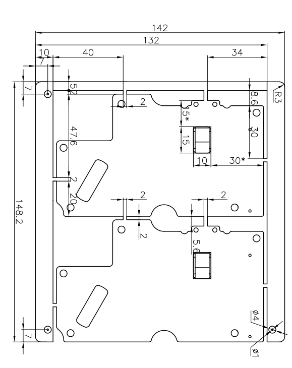
Comparison of Differences between IPC2 and IPC3 standards
2024-06-13
Comparison of differences between IPC2 and IPC3 standards for automotive PCBs:
The IPC level reflects the quality level of each type of printed circuit board, and some electronic manufacturers only have the ability to produce IPC first and second le...
view
detail
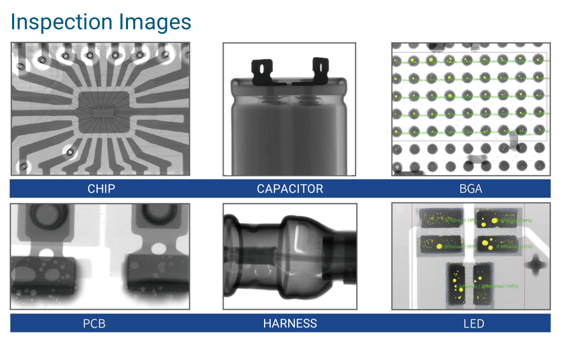
How to identify the invisible defects of PCBA clearly?
2024-06-13
X-RAY Inspection Standards
1. BGA solder joints have no offset:Judgment criteria: acceptable when the offset is less than half of the circumference of the solder pad; When the offset is greater than or equal to half of the circumference of the solder pad, it ...
view
detail
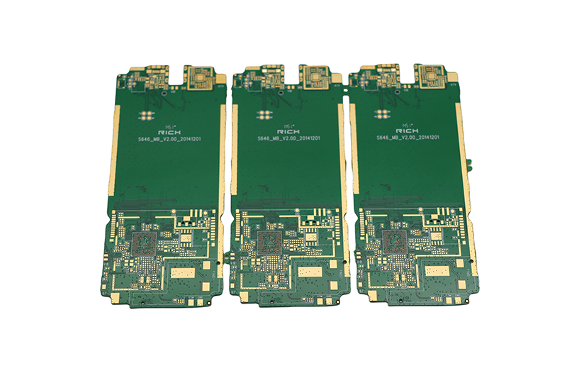
The main difference between HDI and ordinary PCB - a new era of high-density interconnection
2024-06-06
HDI (High Density Interconnection) is a compact circuit board designed for low-volume users. Compared with ordinary PCBs, the most significant feature of HDI is its high wiring density. The difference between the two is mainly reflected in the following four a...
view
detail