As the electric vehicle (EV) industry speeds up toward a greener future, it’s pretty clear that solid infrastructure is more important than ever. At the heart of this is the EV Charging Module PCB Design, which basically acts as the backbone for efficient charging stations. I was chatting with John Smith—he’s a top expert in green tech and the lead engineer over at GreenTech Innovations—and he was saying, “How we design EV charging modules really impacts not just how fast they charge, but also how reliable and long-lasting the whole network is.” That really highlights just how crucial careful design is when it comes to pushing EV infrastructure forward.
Designing these PCBs isn’t as simple as it sounds. There are all kinds of challenges, like managing heat and fighting electromagnetic interference. A well-thought-out PCB is key to making sure charging stations can deliver power quickly and safely—something that’s becoming more critical as more electric vehicles hit the roads. As the infrastructure keeps evolving, using advanced PCB techniques will become a must. It’s definitely shaping up to define the future of electric mobility.
With industries shifting towards cleaner transport options, the importance of smart EV Charging Module PCB design just cannot be overstated. Getting these modules right isn’t just about performance; it’s also about helping more people adopt EVs, taking us a big step closer to a planet that’s a lot greener.
Importance of PCB Design in EV Charging Modules
The significance of PCB design in Electric Vehicle (EV) charging modules cannot be overstated, as it plays a crucial role in ensuring efficiency, reliability, and safety within the rapidly growing EV infrastructure. As reported by the International Energy Agency, the global number of electric cars reached 10 million in 2020, which underscores the increasing demand for effective charging solutions. The design of printed circuit boards (PCBs) in these modules directly influences how energy is transmitted between the charging station and the vehicle, impacting charging times and overall performance.
Moreover, the complexity of EV charging modules necessitates a robust PCB design that can handle high voltages and currents while maintaining optimal thermal management. According to a report by Allied Market Research, the global EV charging infrastructure market is expected to reach $100 billion by 2027. This growing market emphasizes the need for efficient PCB design practices that can accommodate the fast-charging capabilities and advanced communication systems essential for user convenience. With the right materials and layouts, designers can minimize resistive losses, enhance heat dissipation, and ensure electromagnetic compatibility, ultimately leading to safer and more efficient EV charging solutions.
Understanding the Basics of Electric Vehicle Charging Infrastructure
Electric vehicle (EV) charging infrastructure is essential for the successful deployment and adoption of electric vehicles on a global scale. As per a 2021 report by the International Energy Agency (IEA), electric cars could represent up to 30% of the global vehicle fleet by 2030, necessitating a robust and efficient charging network. This growing demand stresses the importance of effective design for EV charging module PCBs (printed circuit boards), which play a critical role in the communication and energy transfer processes during charging.
The foundation of an efficient EV charging infrastructure lies in understanding its components and their interconnections. Charging stations require reliable and high-quality PCBs to manage the various electrical and communication protocols, ensuring fast and safe charging experiences. As noted in a report by Research and Markets, the global electric vehicle charging station market is expected to grow at a CAGR of 34.2% from 2021 to 2028. This exponential growth highlights the need for well-designed PCB solutions that can handle increased power demands and thermal management challenges, ultimately improving the overall efficiency of EV charging systems.
Moreover, the design of these PCBs must prioritize scalability and adaptability to accommodate future technologies and charging standards, such as ultra-fast charging and Vehicle-to-Grid (V2G) capabilities. By investing in innovative PCB designs that are both efficient and versatile, stakeholders can ensure that the necessary infrastructure is in place to support a rapidly evolving electric vehicle landscape.
Key Components of an EV Charging Module PCB Design
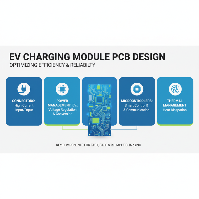
The design of an electric vehicle (EV) charging module PCB (Printed Circuit Board) is essential for optimizing the efficiency and reliability of electric vehicle infrastructure. Key components of a well-engineered EV charging module PCB include connectors, power management ICs, microcontrollers, and thermal management solutions. Each component plays a critical role in ensuring the module can handle the high currents and voltages associated with fast charging while maintaining safety and operational integrity.
Connectors, for example, must be robust enough to support high-frequency data communication as well as high-power transmission, while power management ICs efficiently regulate voltage and current flow to minimize energy loss. According to research from the International Energy Agency, the global EV market is expected to reach over 300 million vehicles by 2040, which underscores the need for advanced charging solutions that can accommodate this rapid growth. Thus, the integration of these components in an effective PCB design directly impacts the overall performance of EV charging stations.
**Tips:** When designing an EV charging module PCB, consider using thermal simulation tools to anticipate heat generation and implement efficient thermal management strategies. Additionally, ensure that layout designs minimize electromagnetic interference (EMI) to enhance reliability and communication efficiency. By focusing on these key areas, manufacturers can significantly improve the functionality and longevity of EV infrastructure.
Design Challenges in EV Charging Module PCBs
The design of printed circuit boards (PCBs) for electric vehicle (EV) charging modules poses several challenges that must be addressed to optimize performance and reliability. One of the primary hurdles is managing the high power density associated with EV chargers. Designers must ensure that the PCB can handle significant current levels while maintaining a compact form factor. This involves careful consideration of trace widths, copper thickness, and thermal management techniques to prevent overheating and ensure efficient power delivery.
Another challenge is electromagnetic interference (EMI), which can seriously impact the performance of charging systems. The compact nature of EV charging modules, combined with high-frequency switching operations, necessitates robust strategies to minimize EMI. Effective grounding techniques, shielding, and the layout of sensitive components can mitigate interference, enhancing the overall stability of the charging process. Additionally, designers must account for the harsh environments that EV charging infrastructure often encounters, ensuring that PCBs are resilient against moisture, temperature variations, and vibration to maintain long-term reliability.
Optimizing PCB Layout for Thermal Management in EV Chargers
The efficiency of electric vehicle (EV) chargers significantly relies on the design of their printed circuit boards (PCBs). In recent years, the demand for EVs has surged, with the International Energy Agency (IEA) reporting a record 10 million EVs sold worldwide in 2022 alone. This increase necessitates robust infrastructure, particularly in the area of charging solutions, where thermal management becomes crucial.
Effective PCB layout directly impacts the reliability and performance of EV chargers, influencing heat dissipation, which is vital for preventing component failure and ensuring long-term durability.
Optimizing the PCB layout for thermal management involves strategic placement of components and the use of advanced materials. According to research published by the Electric Power Research Institute (EPRI), improper thermal management can lead to a reduction in efficiency by up to 20%, negatively affecting charging times and overall user satisfaction. Implementing features such as thermal vias, heat sinks, and careful routing can mitigate these issues.
Additionally, simulation tools can help designers predict thermal behavior, facilitating the creation of a more effective charger layout that meets the increasing power demands of modern EVs. By prioritizing effective thermal management in PCB design, manufacturers can enhance charging efficiency and support the broader adoption of electric vehicles.
Integrating Safety Features in EV Charging Module PCBs
The integration of safety features in EV charging module PCBs is paramount to ensure the reliability and security of electric vehicle infrastructure. As electric vehicle adoption accelerates, charging stations become increasingly critical points in the ecosystem. With the rising number of vehicles on the road, the risk of electrical faults and charging-related incidents also increases. Therefore, incorporating robust safety mechanisms in PCB design is essential to protect both users and equipment.
Key safety features that should be integrated into EV charging module PCBs include overcurrent protection, thermal management, and fault detection systems. Overcurrent protection circuits can prevent damage by cutting off power in the event of excessive current flow, while thermal management solutions, such as heat sinks or thermal pads, help dissipate heat that can arise during prolonged charging sessions. Furthermore, implementing fault detection systems can provide real-time monitoring, allowing the charging station to identify and mitigate potential risks, thereby enhancing user safety and trust in the charging infrastructure.
Overall, the design of EV charging module PCBs with an emphasis on safety features not only improves operational efficiency but also fosters a secure environment for users. This approach not only safeguards expensive equipment but also builds consumer confidence in the electric vehicle ecosystem, paving the way for broader adoption and investment in sustainable transportation solutions.
Future Trends in EV Charging Module Design and Technology
As the electric vehicle (EV) market continues to experience rapid growth, the design of EV charging module PCBs (Printed Circuit Boards) is becoming increasingly crucial. Future trends in EV charging module design are heavily influenced by the need for faster charging solutions and enhanced energy efficiency. Reports indicate that by 2025, the demand for ultra-fast EV charging stations is projected to surge, with a potential market value exceeding $30 billion. Innovations such as integrated circuit designs and advanced thermal management techniques are expected to emerge, significantly improving the performance and reliability of charging infrastructure.
Additionally, the shift towards more sustainable practices has prompted a focus on eco-friendly materials and manufacturing processes in PCB design. The adoption of materials that reduce environmental impact while maintaining high performance is essential. According to a recent study, using renewable resources in PCB production could cut carbon emissions by nearly 50%, aligning the EV industry with global sustainability goals. The integration of smart technology, allowing for real-time monitoring and data collection, is also on the rise, facilitating improved energy distribution and user experience.
**Tips:** When designing EV charging module PCBs, consider prioritizing thermal management solutions to prevent overheating and enhance longevity. Additionally, exploring modular designs can allow for easier upgrades and scalability in response to evolving market demands. Adopting an eco-conscious approach not only helps the environment but can also provide a competitive edge in a rapidly changing landscape.
Why EV Charging Module PCB Design is Critical for Efficient Electric Vehicle Infrastructure - Future Trends in EV Charging Module Design and Technology
| Dimension |
Details |
| PCB Material |
FR-4, High Tg materials |
| Layer Count |
4层到8层 |
| Thermal Management |
使用热沉与导热胶 |
| Size |
100mm x 100mm |
| Connector Type |
Type 1, Type 2, CCS |
| Charging Speed |
22 kW & 150 kW |
| Future Trends |
无线充电, 快速充电网 |
FAQS
: The main components include connectors, power management integrated circuits (ICs), microcontrollers, and thermal management solutions. Each component is essential for handling high currents and voltages safely and reliably.
Connectors are crucial as they must support high-frequency data communication and high-power transmission, ensuring effective performance and safety during charging.
Power management ICs regulate voltage and current flow within the charging module, minimizing energy loss and optimizing overall efficiency.
Key challenges include managing high power density, minimizing electromagnetic interference (EMI), and ensuring resilience against harsh environmental conditions.
Designers should use thermal simulation tools to assess heat generation and implement strategies to manage heat, such as utilizing appropriate trace widths and copper thickness.
Effective grounding techniques, shielding, and careful layout of sensitive components can help reduce EMI, thereby enhancing the stability and performance of charging systems.
It is important to design PCBs that can withstand moisture, temperature variations, and vibration, to ensure they remain durable and functional over time.
The compact design must still accommodate significant current levels without overheating, which requires careful planning and execution of trace design and thermal strategies.
The global EV market is projected to exceed 300 million vehicles by 2040, highlighting the urgent need for advanced and efficient EV charging solutions.
By focusing on components' integration, thermal management, and EMI minimization, manufacturers can significantly enhance both the functionality and durability of EV charging modules.
Conclusion
EV Charging Module PCB Design plays a pivotal role in establishing an efficient electric vehicle infrastructure. The design of printed circuit boards in EV charging modules directly influences the reliability and performance of the entire charging system. Understanding the basics of EV charging infrastructure, including key components and their interactions, is essential for engineers to create effective PCB designs. Various design challenges, such as thermal management and safety features, must be addressed to ensure the longevity and safety of charging stations.
As the demand for electric vehicles continues to grow, optimizing PCB layouts for thermal management becomes increasingly critical. Furthermore, integrating advanced safety features into EV Charging Module PCB Design will enhance user protection and system performance. Future trends indicate a move towards smarter and more integrated EV charging solutions, emphasizing the need for innovative PCB designs that can adapt to evolving technologies and user demands.