Leave Your Message
0%

Lately, HDI PCB electronics manufacturing has really started making waves in the tech world, pushing innovation and making processes way more efficient. I came across a report from ResearchAndMarkets that says the global HDI PCB market could hit around $24 billion by 2026, growing at an average annual rate of about 10.7%. That’s pretty impressive and mostly driven by the huge push for tiny, integrated electronic gadgets now everywhere — from smartphones and laptops to cars and telecom gear. One company that’s leading the charge is Shenzhen Rich Full Joy Electronics Co., Ltd. – they’re actually recognized as a high-tech innovative enterprise here in China. They’re all about using cutting-edge HDI tech in their manufacturing processes. It’s interesting to see how they’ve become a key hub for business incubation, really focusing on pushing the industry forward. They’re continuously improving to keep up with fast-changing tech trends and customer needs, which is pretty exciting to watch as electronics keep evolving at breakneck speed.
7 Reasons Why HDI PCB Electronics Manufacturing is Revolutionizing the Industry

The Shift Towards High-Density Interconnect (HDI) PCBs

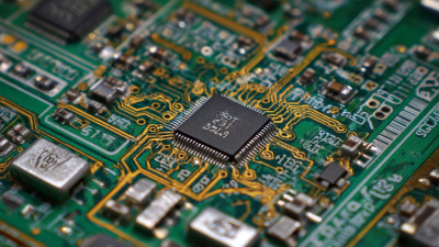
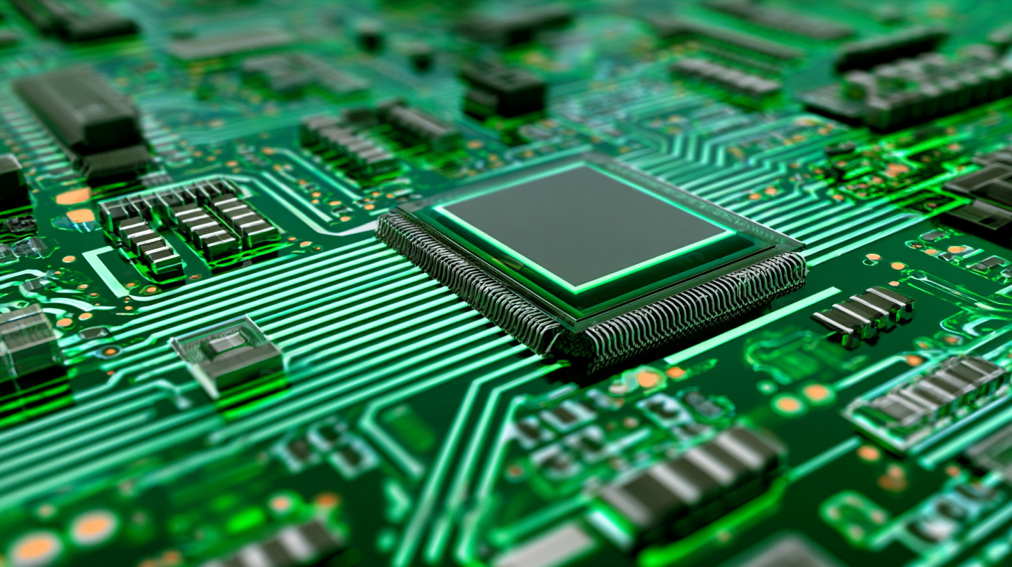
You know, the move toward High-Density Interconnect (HDI) PCBs really marks a big shift in how we make electronics. As gadgets get smaller but more powerful, HDI PCBs come in super handy because they pack more components into tiny spaces without sacrificing performance. But it’s not just about making things smaller — HDI also helps improve signal quality and speeds up data transfer, which is crucial for today's tech like 5G and the Internet of Things.

Getting started with HDI isn’t just a plug-and-play thing, though. It’s smart for manufacturers to invest in top-notch design software that handles complex layouts and helps place components just right. Plus, teaming up with suppliers who really know their stuff when it comes to HDI production can make all the difference, ensuring everything meets industry standards. This kind of collaboration becomes especially important as the industry shifts towards mobile communication and innovation, opening up all sorts of new possibilities.

And don’t forget—the key is to keep your engineering team up-to-date with the latest techniques and materials. Staying in the know about new manufacturing methods means your team can really unlock the full potential of HDI tech. Recognizing these trends and staying ahead of the curve can help companies stay competitive, especially as performance and efficiency aren’t just nice-to-haves anymore—they’re essential for success.
7 Reasons Why HDI PCB Electronics Manufacturing is Revolutionizing the Industry

Innovative Designs: Overcoming Traditional PCB Limitations

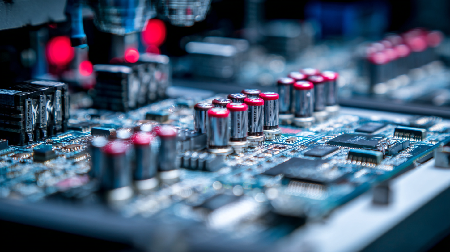
The way HDI (High-Density Interconnect) PCB manufacturing is evolving is really opening up new possibilities for design. We’re seeing these innovative boards that push past the old limitations of traditional PCBs. With stuff like micro-total analysis systems (or µTAS) and lab-on-PCB ideas, manufacturers can now build incredibly compact, efficient solutions that pack multiple functions into just one board. It’s a game-changer because it saves space and boosts the performance of devices, especially in critical areas like medical diagnostics and environmental sensing.

On top of that, the industry is changing fast thanks to new materials and organic electronics. Smaller components mean we can get a lot more creative with design—things that used to be impossible or impractical are now coming to life. 7 Reasons Why HDI PCB Electronics Manufacturing is Revolutionizing the Industry And with the rise of AI and the Internet of Things, these boards aren’t just getting smaller—they’re becoming smarter and more responsive. As we keep moving forward, HDI PCB tech is right at the front, pushing boundaries and helping create some really groundbreaking devices across all sorts of sectors. It’s pretty exciting to see where all this is headed.

Enhanced Performance: The Technical Advantages of HDI Technology

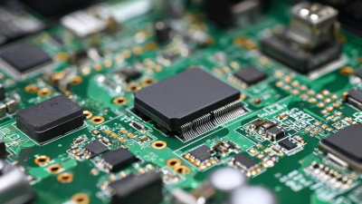
High-Density Interconnect (HDI) tech is really shaking up the world of electronics manufacturing. It offers some pretty awesome advantages that boost both performance and efficiency. One of the coolest things about HDI PCBs is that they can pack in a bunch of dense, functional components within a surprisingly small space. That means you can design much more complex circuits without making the device bigger — perfect for modern gadgets like smartphones, tablets, and other compact electronics.

And get this — HDI uses some pretty advanced manufacturing tricks, like microvias and smarter layer stacking. These help improve signal quality and cut down on electromagnetic interference, which is great because it means devices can run faster and more reliably. As folks keep demanding quicker, more efficient electronics, HDI PCB manufacturing really stands out as a game-changer, stepping up to meet the high standards of today’s tech lovers and industries alike.

Cost-Effectiveness: How HDI PCB Manufacturing Saves Resources

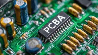
High-Density Interconnect (HDI) PCB manufacturing is really changing the game in the electronics world — and honestly, it’s all about saving costs. By using cutting-edge microvia tech and thinner materials, these HDI boards are a game-changer, making circuits smaller without sacrificing performance. It’s pretty cool how this compact design cuts down on raw materials, which totally helps lower production costs. Plus, the simpler manufacturing steps mean faster assembly and getting products out the door quicker, so companies can focus their resources elsewhere.


If you’re thinking about jumping on the HDI bandwagon and reaping those cost benefits, here are a few tips. First off, try going for multi-layer designs—they pack more components into less space, saving money and boosting performance at the same time. Next, work closely with your PCB suppliers; it helps to team up so you can choose the right materials and design options that fit your budget. And don’t skip good testing and quality checks! Catching problems early on can save a ton of headaches and costs down the line. By adopting these strategies, you’ll make the most out of HDI technology and stay competitive in this fast-changing market.

Sustainability in HDI PCB Production: A Greener Approach

As the electronics world keeps changing, you’ll notice that High-Density Interconnect (HDI) printed circuit boards (PCBs) are really stepping up and helping us move toward a more sustainable future. You know, traditional PCB manufacturing can be pretty resource-hungry and creates a lot of waste, which isn't ideal. But with HDI PCB production, things are different—these advanced techniques use less material while still giving you all the functionality you need. Because of this, we’re seeing smaller, sleeker designs that not only cut down on environmental impact but also save on raw materials.

And it’s not just about being resource-efficient. Companies are really putting effort into making their HDI PCB manufacturing greener, using eco-friendly materials and better processes that follow strict environmental rules. Think lead-free solder, recyclable substrates, and steps to lower energy use during production. All of this means that integrating eco-conscious practices isn’t just good for the planet; it also helps tech companies meet the rising demand for greener electronics. Basically, it’s a win-win—making the industry more responsible, innovative, and ready for the future.

Market Trends: The Future of HDI PCBs in Electronics Manufacturing

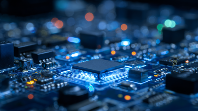
You know, the rapid progress in electronics manufacturing is really being driven by the big jump in demand for High-Density Interconnect (HDI) printed circuit boards. As gadgets get smaller, sleeker, and packed with more features, manufacturers are pretty much turning to HDI PCBs to keep up with what the market wants. They’re packing in cool stuff like microvias, buried and blind vias, plus stacking more layers— all of which boosts performance even in tiny spaces. It’s pretty exciting how this tech isn’t just making devices better but also stretching what’s possible in terms of design and functionality.

And it’s not just about performance. These days, there’s a noticeable shift toward making things more eco-friendly and sustainable in HDI PCB production. More and more, manufacturers are adopting green practices—things like cutting down on waste and using recyclable materials—because consumers are really paying attention to environmental responsibility. This trend lines up with the bigger push for sustainability across pretty much all industries. So, HDI PCBs aren’t just changing the game in electronics—they’re also helping out the planet. Looking ahead, with all the ongoing tech breakthroughs, it’s safe to say HDI is going to continue shaping the future of electronics manufacturing, leading to even more innovative and efficient solutions.

Innovative Custom PCB & PCBA Solutions for Enhanced Performance in Advanced Camera Image Processing

In the rapidly evolving world of camera technology, the demand for high-speed and high-resolution imaging is at an all-time high. Our innovative custom PCB and PCBA solutions are specifically engineered to meet the rigorous demands of advanced camera image processing. By seamlessly integrating with FPGA technologies, our designs offer the capability for real-time image processing, which is essential for a variety of industries including industrial automation, security, and automotive imaging.

The enhanced performance provided by our PCB and PCBA solutions enables manufacturers to push the boundaries of image quality and processing speed. This is particularly important in security applications where capturing high-resolution images swiftly can make the difference in critical situations. Similarly, in the automotive sector, our custom solutions support sophisticated imaging systems that are becoming essential for advanced driver-assistance systems (ADAS) and autonomous vehicles. Our products ensure reliability and performance, allowing developers to implement cutting-edge technology with confidence.

By leveraging our expertise in PCB and PCBA integration, businesses in fields like medical technology can also benefit from improved high-resolution image processing capabilities. As the resolution and speed of imaging systems grow, our tailored solutions stand out as a vital component in achieving unmatched performance, paving the way for innovations that enhance safety, efficiency, and functionality across various applications.

FAQS

: What is HDI PCB technology?

: HDI (High-Density Interconnect) PCB technology refers to advanced printed circuit board manufacturing that utilizes microvia technology and thinner materials to create compact and efficient designs with enhanced performance.

How does HDI PCB manufacturing impact the electronics industry?

HDI PCB manufacturing transforms the industry by reducing circuit board sizes, minimizing material usage, decreasing production costs, and streamlining manufacturing processes, which enhances overall efficiency.

What are the benefits of integrating HDI PCBs in electronic devices?

The integration of HDI PCBs allows for the creation of compact solutions that combine multiple functionalities into a single board, improving performance and saving space in critical applications like biomedical diagnostics and environmental monitoring.

What strategies can businesses use to leverage cost-saving benefits from HDI PCB manufacturing?

Businesses can adopt multi-layer designs, collaborate closely with PCB manufacturers for better material selections and design choices, and implement rigorous testing and quality control to minimize costs and maximize investment.

How does the miniaturization of components in HDI PCBs influence design capabilities?

The miniaturization of components allows for more intricate designs that were previously impractical, enabling manufacturers to create highly compact and efficient electronic solutions.

What role do advanced materials and organic electronics play in HDI PCB technology?

Advanced materials and organic electronics are driving significant changes in the HDI PCB industry, facilitating the miniaturization of components and enabling more sophisticated and efficient designs.

How does the trend toward smart systems relate to HDI PCB technology?

The integration of artificial intelligence and the Internet of Things with HDI PCB technology allows for the development of smarter, more responsive systems that enhance the capabilities of electronic devices across various sectors.

In what applications are HDI PCBs particularly beneficial?

HDI PCBs are particularly beneficial in critical applications such as biomedical diagnostics and environmental monitoring where compactness and performance are essential.

What are micro-total analysis systems (µTAS)?

Micro-total analysis systems (µTAS) are integrated lab-on-PCB concepts that allow for compact and efficient electronic solutions capable of performing multiple functions within a single board.

How can close collaboration with PCB manufacturers improve cost efficiency?

Close collaboration with PCB manufacturers can lead to better material selections and design choices that align with the company's budget, ultimately enhancing cost efficiency during the production process.

Conclusion

The world of electronics manufacturing is really changing these days, mostly thanks to HDI PCB technology. As industries pivot toward High-Density Interconnect PCBs, we’re starting to see some pretty innovative designs popping up that actually get around the usual limitations. It’s not just about better performance—though that’s a big plus—it’s also about saving costs and resources, which is a huge win for everyone. Companies like Shenzhen Rich Full Joy Electronics Co., Ltd. are leading the charge here, showing how focus and expertise can come together to push high-tech boundaries.

Plus, there’s a big focus on sustainability, which is super important. The process behind making HDI PCBs is becoming more eco-friendly, helping the industry move towards greener practices. Looking ahead, with more companies adopting HDI tech, the future of electronics manufacturing looks pretty promising—more efficient, effective, and kinder to our planet. Getting on board with these advances isn't just smart for business; it helps companies stay competitive and meet the changing needs of consumers all over the world.

Clara

Clara

Clara is a dedicated marketing professional at Shenzhen Ruizhi Xinfeng Electronics Co., Ltd., where she leverages her extensive knowledge of the company's products to drive marketing initiatives. With a focus on excellence, she regularly updates the company’s professional blog, sharing insights......
Previous Future Trends in High Frequency Pcb Technology for Global Buyers