You know, as the electronics world keeps changing so fast, everyone’s really hungry for smaller, more powerful circuit boards. That’s why HDI PCB fabrication is getting a lot of attention these days. But honestly, the old-school methods might not cut it anymore when it comes to the cutting-edge stuff out there. In this post, I want to share some fresh, innovative alternatives to how we make HDI PCBs—they not only boost how well things work and how reliable they are, but they also help your designs stay ready for whatever new tech comes along.
Over here at Shenzhen Rich Full Joy Electronics Co., Ltd., we’re a high-tech company that’s proudly pushing the boundaries of what's possible, with a real focus on innovation. We get how crucial it is to keep evolving how we produce these boards so you can stay ahead in a pretty competitive market. So, stick around as we explore some game-changing solutions that’ll help your electronics stay awesome and relevant, no matter how crazy the tech world gets.
The Limitations of Traditional HDI PCB Fabrication Methods
You know, traditional HDI (High-Density Interconnector) PCB manufacturing has been pretty much the backbone of today’s electronics. It’s what made smaller, more powerful gadgets possible. But, honestly, those methods aren’t perfect—costs can add up, and scaling up isn’t always straightforward. According to a report from IPC, the global PCB market is expected to hit around $76 billion by 2024, and a big chunk of that is thanks to HDI tech. Still, as demand keeps growing, these older processes just can’t keep pace with how fast the industry is changing. That often means longer wait times and production costs going through the roof.
Plus, designing HDI boards isn’t exactly a walk in the park. They usually need multiple layers and tiny microvias, which makes manufacturing tricky—think more chances for errors, less consistency, and reliability issues. Research and Markets even pointed out that defect rates for HDI PCBs can hit up to 10%. That’s a big deal because it affects how many good units you get and can really drive up costs overall. All of this just shows that we need new, smarter ways to make these boards—methods that are more efficient, sustainable, and cheaper in the long run. Things like additive manufacturing or using new materials might just be the game-changers we’ve been waiting for, helping us create the next generation of PCBs that can handle whatever the market throws at us.
Emerging Technologies Transforming PCB Production
The world of PCB manufacturing is really going through some exciting changes right now. New tech is popping up that could totally change how we make circuit boards. You know, traditional methods have their limits—things like flexibility, environmental impact, and how easily they can be scaled up. But with things like 3D printing and additive manufacturing getting better, manufacturers can now craft really complex circuit designs way more efficiently. Plus, these new methods help make circuits that are lighter and more compact, which is a big deal given how fast electronics are evolving.
And it’s not just the printing tech. New materials are shaking things up too. We’re talking about new kinds of substrates and conductive inks that don’t just boost performance—they also cut costs. These materials are tougher too—they can handle higher heat and electrical loads—making them perfect for high-end stuff like electric vehicles and IoT gadgets. Also, incorporating smart tech into the manufacturing process makes everything run smoother—faster production times and better quality control, no doubt. As these innovations keep advancing, it’s pretty amazing to think about how they’ll redefine what’s possible in PCB making, paving the way for more future-proof solutions in our increasingly digital world.
Exploring Innovative Alternatives to Hdi Pcb Fabrication for Future Proof Solutions - Emerging Technologies Transforming PCB Production
| Technology |
Description |
Advantages |
Application Areas |
Development Stage |
| Additive Manufacturing |
3D printing technology utilized for PCB fabrication, allowing for complex geometries. |
Reduced material waste, faster production times. |
Consumer electronics, IoT devices, automotive. |
Research and Development |
| Flexible PCBs |
PCBs that can bend and flex, accommodating compact designs. |
Lightweight, innovative design possibilities. |
Wearable technology, medical devices, mobile phones. |
Commercial |
| Embedded Components |
Components embedded within the PCB substrate to save space. |
Space-efficient designs, improved performance. |
Smartphones, tablets, automotive electronics. |
Pilot Production |
| High-Density Interconnect (HDI) |
PCBs with significantly higher wiring density than traditional PCBs. |
Smaller, more efficient devices. |
Networking equipment, advanced communication devices. |
Mature |
Sustainability in PCB Manufacturing: Eco-Friendly Alternatives
As the electronics world keeps on evolving, sustainability is becoming a pretty big deal when it comes to making printed circuit boards, or PCBs for short. You see, the traditional ways of making high-density interconnect (HDI) PCBs often use materials and processes that aren’t exactly eco-friendly. That’s why folks are now on the lookout for greener options—things that not only do the job technically but also care about the environment. We’re seeing some pretty exciting innovations, like biodegradable substrates and non-toxic inks, helping push manufacturing towards more eco-conscious practices.
Plus, recycling and reusing parts are gaining serious ground. It’s a smart way to cut down on waste and reduce the need for new, raw materials. Then there’s this cool tech called additive manufacturing—think of it like building PCs layer by layer—which can really cut down on material waste and energy use. Bottom line? By embracing these sustainable tricks, the industry is taking meaningful steps toward future-proofing itself—making sure that as we meet tomorrow’s tech demands, we’re also doing right by the planet. It’s all about finding that balance, you know?
Comparative Analysis of HDI and Innovative PCB Techniques
The world of printed circuit boards (or PCBs, as everyone else calls 'em) is changing pretty fast these days, especially with the surge in High-Density Interconnect technology—HDI for short. If you’ve been watching the market, you’ll notice it’s exploding, mainly because everyone’s looking for smaller, sleeker designs in gadgets, cars, and all that tech stuff. In fact, recent reports say the automotive industry’s gonna play a huge role here, using HDI boards for stuff like advanced driver-assistance systems (you know, those fancy safety features) and electric vehicles. These boards are crucial because they allow for much finer line widths and tighter spacing—pretty much the backbone for high-performance tech devices.
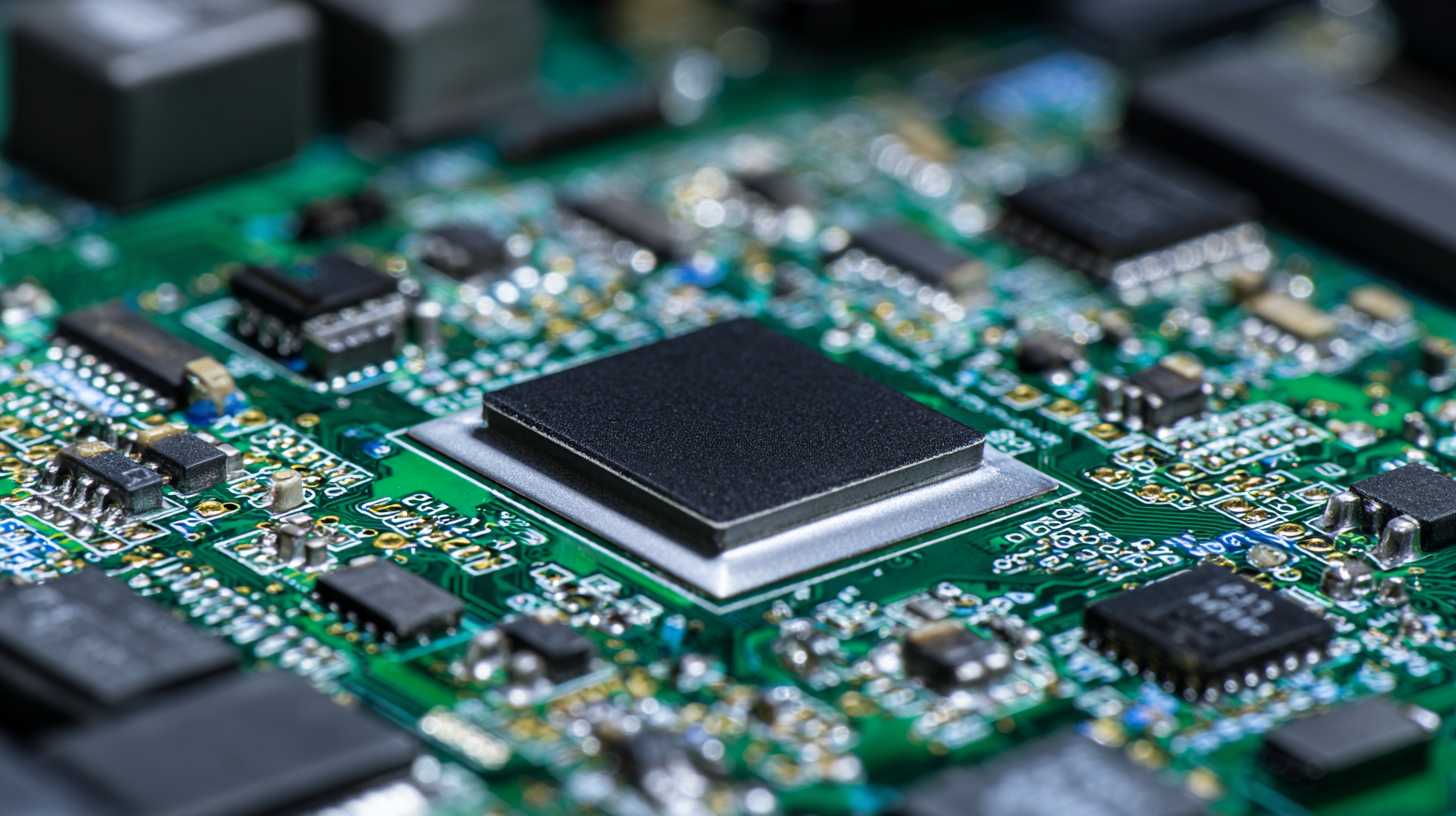
But it’s not just HDI boards stealing the show. Other methods, like flexible PCBs and the traditional multi-layer rigid boards, are also gaining ground because they each bring their own set of perks to the table. For example, the market for LDI exposure machines—which are kinda like the printers for PCBs—is expected to grow from around $873 million in 2025 to over $1.15 billion by 2033. That’s a clear sign that the industry’s moving towards more innovative fabrication tech. All in all, this shift reflects just how complex electronics are getting and underscores the need for future-proof solutions to keep up with how fast technology’s evolving.
Future Trends: Anticipating Needs in PCB Design and Fabrication
The world of PCB design and manufacturing is changing pretty fast these days, mainly because of new tech developments and the growing demands from different industries. If you look at the global printed circuit board market, it’s expected to really take off—from about $69.7 billion in 2023 to around $113.5 billion by 2032. So, it’s more important than ever to stay on top of what’s next in this field. Industries like automotive and electronics are all about making smaller, more efficient devices, which means there’s a real push for new and better PCB options. Plus, with generative AI gaining ground, the whole semiconductor industry is poised for a shake-up, pushing us to innovate faster to meet those new challenges.
Events like IMPACT 2023 really drive home just how critical advanced packaging and the latest tech are for PCB production today. Takeaways from these kinds of conferences show the industry is moving toward multi-layered boards and complex assemblies—stuff that can handle super sophisticated electronic applications. Companies aren’t just responding to what’s needed right now—they’re planning ahead, trying to stay flexible and ready for whatever the future might bring in PCB design and manufacturing. Looking at those market growth predictions, it’s clear that continuing to develop innovative, future-proof PCB solutions will be a top priority for everyone involved in making electronics. It’s an exciting time, with a lot of change on the horizon!”
Exploring Innovative Alternatives to Hdi Pcb Fabrication
Practical Applications of New PCB Technologies in Modern Electronics
You know, the way PCB tech has been evolving lately is pretty exciting. It's like opening up a whole new world for modern electronics—products are not just getting more efficient, but also way more versatile. Stuff like flexible PCBs and embedded components are really shaking things up in design. These alternatives to the traditional HDI PCBs give manufacturers the chance to craft compact devices that can squeeze into tight spaces—think wearables or IoT gadgets. And the best part? Being able to shape circuits to match different forms opens up all sorts of cool design possibilities, making products both look better and work better—pretty much exactly what consumers want these days.
Plus, there’s this push really happening with new materials—like high-frequency substrates and eco-friendly laminates—that’s pushing sustainability forward. It’s not only about boosting performance in high-speed apps but also about being kinder to the environment. By jumping on these innovative PCB tech trends, companies can keep their products relevant and stand out in this crowded market. As folks keep demanding smarter, smaller, and more efficient electronics, embracing these new fabrication methods is pretty much essential if you want to stay ahead of the game and give users a better experience overall.
Understanding the Role of High-Quality PCB Assembly in Medical Devices: Insights from Recent Industry Reports on Quality Standards and Market Trends
In the realm of medical devices, the integrity of printed circuit board (PCB) assembly is paramount. According to recent industry reports, the demand for high-quality PCB assembly in medical applications is projected to grow significantly, driven by advancements in technology and the increasing need for reliable medical solutions. A report from Market Research Future indicates that the global market for medical electronics will reach $60 billion by 2027, emphasizing the critical role of PCB assembly in ensuring device effectiveness and safety.
Richpcba stands out in this competitive landscape, offering specialized PCB assembly services tailored to the medical sector. Our commitment to quality begins with strict adherence to industry standards, which is essential given the high stakes involved in medical applications. We utilize a combination of automated, hybrid, and manual manufacturing processes to achieve the accuracy required for medical devices. This flexibility in production methods enables us to meet diverse demands while maintaining exceptional quality.
Moreover, as electronic devices become increasingly sophisticated, the complexity of PCB design and assembly continues to grow. This is underscored by a report from the IPC (Association Connecting Electronics Industries), which notes that 78% of medical device manufacturers cited quality assurance as their top concern in PCB assembly. By partnering with Richpcba, clients benefit from our expertise in navigating these complexities, ensuring that their medical devices are not only compliant with regulations but also equipped to perform reliably in critical scenarios.
FAQS
: Eco-friendly alternatives in PCB manufacturing include biodegradable substrates and non-toxic inks, which help to reduce environmental harm while meeting technological demands.
Recycling and reusing components reduce waste and minimize the need for virgin materials, contributing to more sustainable manufacturing practices in the electronics industry.
HDI technology refers to a type of printed circuit board that allows for finer line widths and spacing, enabling compact designs essential for high-performance devices, particularly in consumer electronics and automotive applications.
The automotive sector is a major contributor to the growth of HDI PCBs, utilizing them for advanced driver-assistance systems (ADAS) and electric vehicle (EV) technologies.
Alternative techniques include flexible PCBs and traditional rigid multilayer boards, each offering unique advantages for various applications.
Generative AI is anticipated to reshape the semiconductor industry, creating a need for rapid innovation in PCB capabilities to meet emerging requirements.
The global printed circuit board market is projected to grow from $69.69 billion in 2023 to $113.49 billion by 2032.
The focus on multilayer boards is due to their ability to accommodate sophisticated electronic applications, reflecting the industry's shift towards more complex assemblies.
Events like IMPACT 2023 are significant as they highlight advancements in packaging and technologies integral to PCB fabrication, emphasizing the industry's response to current and future needs.
Companies are strategically planning to anticipate future requirements by focusing on adaptability and resilience in their manufacturing processes, ensuring they can meet the evolving demands of technology.