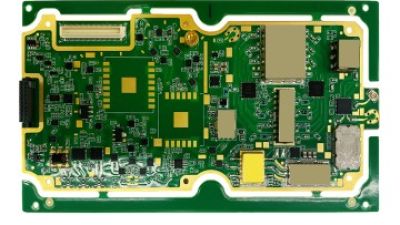
High-frequency PCB design is pretty crucial in today’s electronics world. Experts often stress how important it is to have a solid, efficient design to hit performance goals. I remember John Smith from High-Frequency PCB Solutions once saying, *
Understanding High Frequency PCBs: Definition and Importance
High-frequency printed circuit boards (PCBs) are crucial in modern electronics. They facilitate effective signal transmission at elevated frequencies. Typically, high-frequency PCBs operate above 1 GHz, suitable for applications in telecommunications, radar, and satellite systems. A shift towards 5G technology has increased their importance. The demand for higher bandwidth and reduced signal loss is driving the industry forward.
According to a report by Mordor Intelligence, the global high-frequency PCB market is projected to grow at a CAGR of 6.2% from 2021 to 2026. This growth is fueled by advancements in wireless technology and IoT applications. However, designing these PCBs is challenging. Factors like material selection and trace width are critical for minimizing losses. Engineers often face difficulties in balancing performance with manufacturing costs. Choosing the right dielectric materials, such as PTFE, can significantly impact the board's efficiency, but they can also be more expensive and harder to source.
Moreover, signal integrity is a major concern. Inadequate designs can lead to reflections and interference. Many designs fail to account for these issues, resulting in inefficient performance. Engineers are learning the importance of simulation tools to predict the behavior of high-frequency signals on PCBs. While prototypes can solve some issues, the cost and time of revisions can be substantial. This highlights the ongoing need to refine design processes and improve methodologies in the industry.
Key Design Principles for High Frequency PCB Efficiency
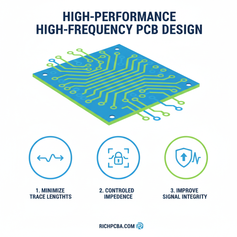
When designing a High-Performance High-Frequency PCB, attention to detail is crucial. Start by minimizing the length of traces. Shorter traces reduce parasitic capacitance and inductance, leading to better signal integrity. Use controlled impedance to ensure signals travel efficiently. This helps in maintaining signal quality at high frequencies.
Layer stack-up is another important aspect. Utilizing multiple layers can help manage the return paths for high-frequency signals. Pay attention to ground planes. A solid ground plane can reduce noise and improve overall performance. However, avoid making the ground plane overly complex, as it may introduce new challenges.
Lastly, consider component placement carefully. Place sensitive components away from high-frequency signal paths. This reduces interference and enhances performance. It's essential to test designs thoroughly. Issues often arise that weren’t anticipated during the design phase. Being open to revisiting and refining your design is key to achieving efficiency in high-frequency applications.
Material Selection for Optimal High Frequency PCB Performance
When designing high-frequency PCBs, material selection is critical. You want materials that can handle high speeds and minimize signal loss. A common choice is the
High-Frequency High-TG Material.
Its high glass transition temperature makes it stable under heat. This stability is essential for maintaining performance during operation.
Using the right laminate can significantly affect the board's performance. For instance, Teflon-based materials are excellent for RF applications. However, these materials can be tough to process.
Some boards may suffer from delamination if not handled properly. Design teams sometimes overlook the impact of dielectric constant and loss tangent in their calculations.
This oversight can lead to inefficiencies.
Another aspect to consider is the thickness of the materials. A thicker dielectric may reduce loss, but it can also increase the size of the PCB. Striking a balance is key. Engineers often experiment with different combinations.
They seek the design that provides the best performance without unnecessary complexity. A carefully chosen material will lead to a more reliable and efficient PCB design.
Layout Techniques to Minimize Signal Loss in High Frequency PCBs
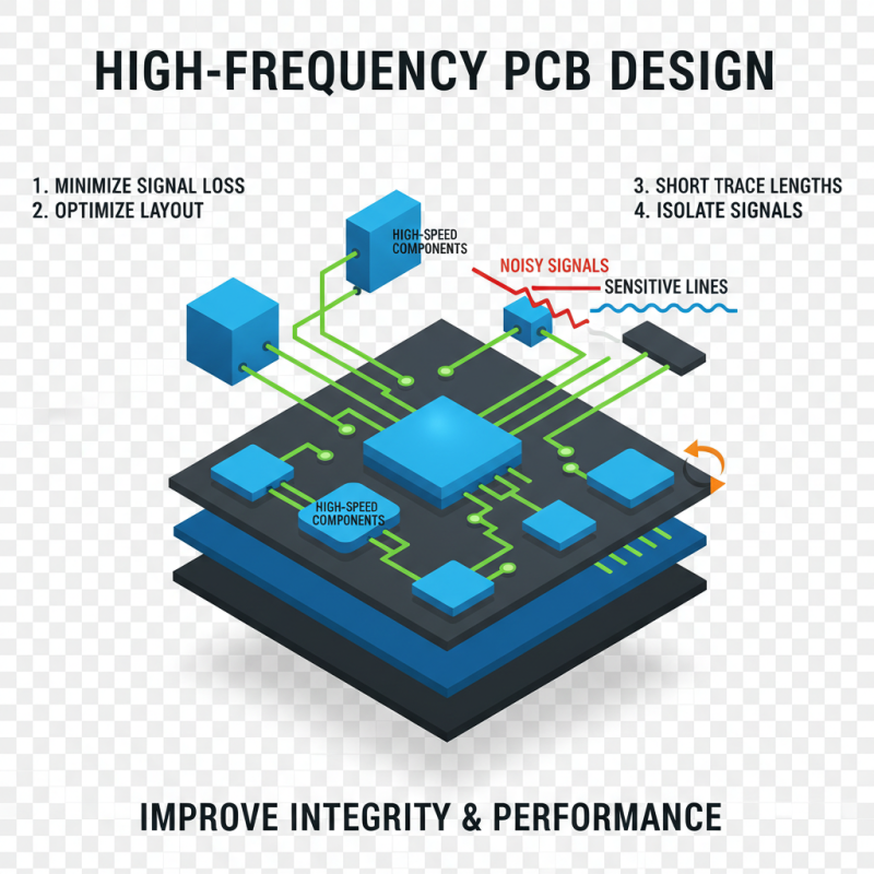
In high frequency PCB design, minimizing signal loss is crucial. Layout techniques play a key role. Pay attention to the placement of components. Arrange them to reduce the length of high-speed traces. Keep sensitive lines away from noisy signals. This helps maintain integrity and performance.
Another important tip is to use proper grounding. A solid ground plane shields sensitive components. It also minimizes interference. Ensure that vias are short and direct. Unnecessary connections can add capacitance and inductance, leading to signal degradation.
Remember to consider impedance matching. This prevents reflections that can corrupt signals. Use controlled impedance traces for effective communication. Make adjustments based on the stack-up configuration. Don't overlook the importance of these details. Each choice impacts the final design. High frequency PCBs require careful thought and constant reflection.
Thermal Management Strategies in High Frequency PCB Design
Thermal management in high frequency PCB design is crucial. High frequencies generate significant heat, impacting performance. Effective cooling strategies are essential for functionality. Using thermal vias can help. They channel heat away from critical components and distribute it evenly. Proper placement of these vias is important. However, it may not always solve heat issues completely.
Another strategy involves using thermal pads and heatsinks. These components absorb and dissipate heat effectively. While beneficial, they require additional space on the board. It can complicate design layouts. Engineers often face challenges when balancing thermal management with other PCB constraints.
Heat spreaders can also play a role. They distribute heat across a broader area, reducing hotspots. Yet, selecting the right material is vital. Some materials can increase weight and cost. Designers should reevaluate their choices as they develop prototypes. Ultimately, the goal is to achieve an optimal balance between performance and thermal efficiency. Conducting thorough testing is necessary. This ensures reliability in the final product.
High Frequency PCB Tips for Efficient Design and Applications
| Tip |
Description |
Application |
Thermal Management Strategy |
| Layer Stack-Up Optimization |
Optimize the arrangement of layers to reduce signal integrity issues. |
High Speed Digital Circuits |
Use of vias and ground planes to dissipate heat. |
| Minimize Signal Paths |
Shorten the distance of signal paths to reduce electrical noise. |
Radio Frequency Applications |
Cooling techniques such as airflow management. |
| Use Controlled Impedance |
Design traces with specific dimensions to maintain signal integrity. |
High-Frequency Communication |
Implement heat sinks for components. |
| Thermal via Placement |
Strategic placement of thermal vias to transfer heat away from components. |
Power Amplifiers |
Use of thermal pads on PCB and components. |
| Material Selection |
Choose materials based on thermal conductivity and dielectric constant. |
High-Frequency Applications |
Use of advanced cooling techniques like Peltier elements. |
Testing and Validation Methods for High Frequency PCB Applications
When developing high-frequency PCBs, effective testing and validation are crucial. High-frequency PCBs differ significantly from regular PCBs. The materials used, such as low-loss substrates, directly impact performance. Testing these designs requires specialized equipment. Standard tools may not provide the necessary accuracy needed for high-frequency signals.
One common method is vector network analysis. This technique measures S-parameters to assess how signals behave at different frequencies. Proper validation can reveal issues early in the design process. It's essential to conduct real-world tests under varied conditions. High-frequency applications often face challenges, such as signal integrity and electromagnetic interference. Engineers should not overlook these factors.
Another method involves time-domain reflectometry. This helps identify faults in the PCB layout. It’s a helpful approach but can be complex. Sometimes, the results can be misleading, requiring careful interpretation. Clear documentation of tests and designs aids in troubleshooting. A robust validation process enhances reliability. Ultimately, understanding the difference between a high-frequency PCB and a regular PCB is vital for success.
Future Trends in High Frequency PCB Technologies and Applications
The landscape of high-frequency PCB technologies is evolving rapidly. Increasing demand for wireless communication pushes engineers to innovate. Emerging materials are being explored to enhance signal integrity and reduce losses. These materials often come with their own challenges. For instance, cost and availability can be significant factors. Ensuring consistency in manufacturing remains a hurdle.
Another trend is the miniaturization of electronic devices. This shift requires Hf PCB designs to be more compact without sacrificing performance. Compact designs can lead to higher heat levels. Balancing size and thermal management becomes crucial. Some designs may overlook the impact of thermal stress. Engineers need to reflect on these aspects during the design phase.
Artificial intelligence is also making waves in high-frequency PCB design processes. AI algorithms can optimize layouts for efficiency. However, reliance on technology could lead to overconfidence. Engineers should maintain their critical thinking skills. The future of Hf PCB technology promises advancements, but it will require careful navigation of these complexities.
High Frequency PCB Applications and Efficiency Trends
Leveraging Industry Insights: High-Frequency RF PCB and PCB Assembly Technologies for Enhanced Performance in Advanced Electronics
In the rapidly evolving landscape of advanced electronics, the demand for high-frequency RF PCB and PCB assembly technologies is more critical than ever. As industries such as telecommunications, military, and aerospace push for greater performance, the reduction of signal loss in RF circuits has become a key focal point. According to a recent report by the International Electrotechnical Commission (IEC), the RF PCB market is expected to witness a compound annual growth rate (CAGR) of 14.5% through 2027, underscoring the need for precision-engineered solutions that can meet stringent operational requirements.
With over 20 years of expertise in RF PCB manufacturing, companies are increasingly turning to turnkey PCB assembly services that not only ensure high performance but also expedite production timelines. The importance of using low-loss materials and advanced fabrication techniques cannot be overstated, as these factors significantly influence the efficiency and reliability of RF circuits. Industry insights indicate that manufacturers adopting cutting-edge technologies like multilayer PCBs and advanced dielectric materials can achieve up to 30% reduction in signal loss, which is paramount in high-frequency applications.
Moreover, as the complexity of electronic devices continues to rise, so does the necessity for innovation in PCB assembly processes. Flexibility in design, coupled with precise engineering, enables the production of compact and lightweight PCBs that can withstand extreme conditions, particularly in military and aerospace applications where performance and durability are non-negotiable. Leveraging industry insights and advancements in high-frequency RF technology, manufacturers are well-positioned to enhance the capabilities of next-generation electronic systems.
FAQS
: The product improves daily efficiency. It enhances focus and boosts productivity. Many users report feeling more energized.
Use it as directed. Consistency is key. Incorporate it into your routine for maximum effectiveness.
Some users may experience mild discomfort. Reactions vary from person to person. It's wise to monitor how you feel.
Consult a healthcare professional first. Allergies can affect tolerance. Ensure it’s safe for your specific situation.
Results can vary greatly. Some notice changes within days. Others may take weeks to experience benefits.
Reach out for support. They may offer solutions. Feedback is valuable for both users and producers.
Yes, follow the suggested guidelines. Taking too much can lead to issues. It’s better to start slow and adjust.
Conclusion
High Frequency PCBs are crucial in modern electronics, where signal integrity and efficiency are paramount. Understanding their definition and significance is the first step towards mastering their design. Key design principles include minimizing signal loss through careful layout techniques and selecting materials that enhance performance at high frequencies.
Additionally, effective thermal management strategies play a significant role in high frequency PCB design, ensuring that devices can operate safely and effectively under varying conditions. Testing and validation methods are essential to confirm the reliability of high frequency PCB applications. Looking ahead, emerging trends in high frequency PCB technologies promise to further improve performance and adaptability in a range of industries.