Complete Guide to PCB Manufacturing Process | HDI PCB Production Explained
Behind every reliable electronic device lies a meticulously manufactured printed circuit board (PCB). From 5G infrastructure to automotive electronics, medical devices, and consumer gadgets, PCBs form the backbone of electronic systems. Understanding the detailed production process is crucial for design engineers, quality managers, and procurement professionals aiming for high performance and reliability.
In this article, we unveil the comprehensive PCB manufacturing process, from inner layer imaging to final inspection. We also explore special HDI (High-Density Interconnect) processes that enable higher routing density and smaller form factors.
Standard PCB Manufacturing Process: Key Steps Explained
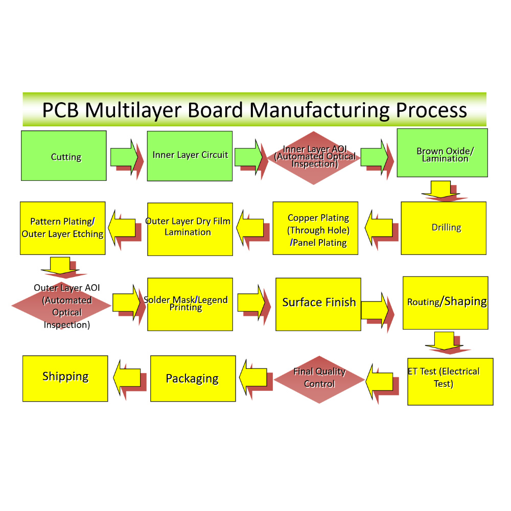
1. IL Image (Inner Layer Imaging)
Circuit patterns are transferred onto the inner copper layers using photolithography techniques, forming the foundational traces for multilayer PCBs.
2. I/L AOI (Inner Layer Automated Optical Inspection)
High-resolution AOI machines inspect inner layers for shorts, opens, and pattern defects, ensuring accurate circuitry before lamination.
3. B/Oxide (Black Oxide or Oxidation Treatment)3. B/Oxide
An oxide or black oxide coating is applied to the inner copper surfaces to enhance adhesion with prepreg layers during lamination.
4. Layup
The inner layers, prepreg (semi-cured resin), and outer copper foils are stacked according to the design to prepare for multilayer bonding.
5. Press (Lamination)
The stack is subjected to high temperature and pressure in a lamination press, fusing the layers into a solid multilayer PCB core.
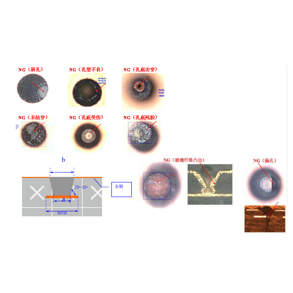
6. Laser Drilling
Microvias are drilled with lasers to connect outer layers to specific internal layers, essential for fine-pitch BGA(超链接:https://www.richpcba.com/bga-assembly-capability/ ) and HDI designs.
7. Drilling (Mechanical)
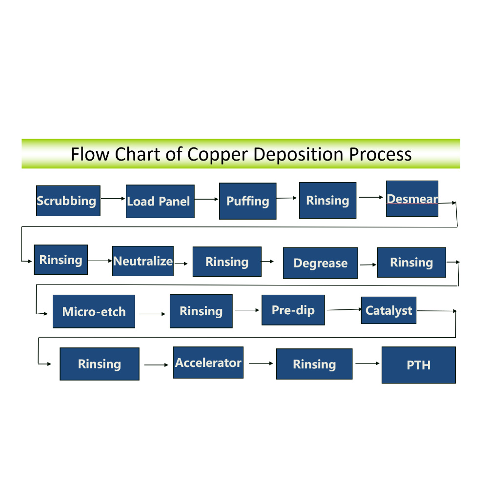
8. PTH (Plated Through Hole)
Through-holes are chemically and electrolytically plated with copper to establish electrical interconnects across multiple layers.
9. Panel Plating
A full-panel copper plating step increases the thickness of conductive paths and ensures uniform metallization across drilled holes.
10. O/L Image (Outer Layer Imaging)
Circuit patterns are transferred to the outer copper foils using photoresist and UV exposure, similar to inner layer imaging.
11. Pattern Plating
Selective copper plating reinforces areas that form the circuit traces while non-essential copper is removed in the next step.
12. SES Etching
Chemical etchants dissolve unprotected copper, leaving behind precise circuit features that match the design layout.
13. O/L AOI (Outer Layer AOI)
The outer layers undergo another round of automated optical inspection to detect any defects like opens, shorts, or misalignments.
14. S/Mask (Solder Mask Application)
A solder mask ink is applied and patterned via exposure and development to protect the board from oxidation and prevent solder bridges during assembly.
15. Legend (Silkscreen Printing)
Component identifiers, logos, and reference designators are printed to assist in assembly, testing, and servicing.
16. Surface Finish (Surface Treatment)
Left Branch (High-End Finishes):
●ENIG (Electroless Nickel Immersion Gold)
●ENEPIG (Electroless Nickel Electroless Palladium Immersion Gold)
●Hard Gold, Soft Gold
●HASL (Hot Air Solder Leveling) and LF-HASL (Lead-Free)
These finishes enhance solderability, oxidation resistance, and wire bonding compatibility.
Right Branch (Alternative Finishes):
●Immersion Tin, Immersion Silver
●OSP (Organic Solderability Preservatives)OSP
These are cost-effective and suitable for RoHS-compliant applications.
17. Rout (CNC Profiling)
Using CNC routers or V-cut machines, the PCB is milled to its final outline and separated into individual boards.
18. ET (Electrical Testing)
Comprehensive open/short tests ensure that all circuits are properly connected and there are no electrical defects.
19. FV (Final Visual Inspection)
Skilled inspectors perform a manual quality check to identify any visual defects or inconsistencies before shipping.
HDI PCB Manufacturing: Enhanced Steps for High-Density DesignsHDI PCB
HDI (High-Density Interconnect) PCBs go beyond standard manufacturing processes by enabling ultra-fine lines, microvias, and compact form factors required in smartphones, IoT devices, and advanced computing.
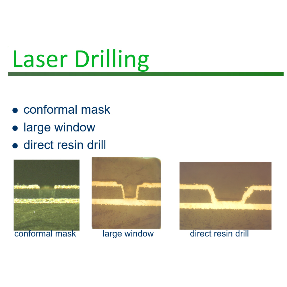
Additional Layer-Building Processes
1. Dielectric Coating for Build-Up Layers
2. Laser Drilling of Blind Vias
3. Blind Via Metallization
4. Build-Up Trace Imaging & Etching
5. Repeated Build-Up Cycles